FAQ: Logic and Voltage Translation > Voltage Translators >> Current FAQ
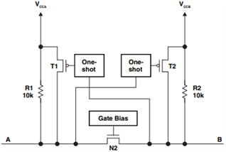
TXS family translators utilize a FET-based architecture with an N-channel pass-gate transistor used to open and close the connection between the A-port and B-port. The FET connects the A and B sides when either input is forced to a voltage less than ~VCCA. With this type of architecture, the output voltage has a direct dependency on the input voltage due to there being a direct connection, unlike with the more traditional buffered architecture seen in most digital devices.

For most system designers, having VOH/VOL specifications is helpful to verify if the down stream devices can properly interpret the logic levels which is why they are included with for the TXS family. Due to the dependency the output voltage has with the input voltage, the VIH/VIL conditions need to be strict to maintain adequate VOH/VOL levels commonly seen with digital devices. For example, the maximum VIL value is provided to ensure that a valid VOL is maintained since VOL is the sum of VIL and the voltage drop across the pass-gate transistor (N2 in the image above).
Having a good understanding on the FET-based architectures will provide more clarity on this matter. These Logic Minute Videos covering the LSF family, a family that also uses the FET-based architecture, do a great job at walking through the functionality. A Guide to Voltage Translation With TXS-Type Translators is another great resource for understanding how the TXS family works.

