This thread has been locked.

If you have a related question, please click the "Ask a related question" button in the top right corner. The newly created question will be automatically linked to this question.

SN74HC165: Is there anyting different in different batch?

Part Number: SN74HC165
Other Parts Discussed in Thread: SN74HCS165

Hi Team,

Customer says there is a Bug when they use SN74HC165 in new batch board.

They read board ID but there is something wrong.The board ID is 10001101, but what they read is 00011011. Following is their schematic.

I test their board in old batch, the waveform is following, the hold time is 14ns. In their board the sample point is the rise edge.

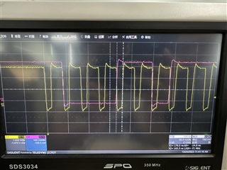
Following is their new batch, the hold time is 11ns. That's the main different between the two batch device. And all the device is customer buy after 2Q2022.

We have advise customer to change the PCB or firmware. But it's difficult for them to change those. 

Is there any other ways to solve that?

Thanks a lot.

  • With a 3.3 V supply, the guaranteed maximum clock frequency is 15.4 MHz. This clock is too fast. (But this device happens to actually work with a higher frequency, so this is not the cause.)

    The problem is that the controller is using a wrong SPI mode. The value of the H input is initially visible at the Q output, and the first rising edge shifts to the next one, the G input. So the SPI master must sample the first bit before the first rising edge. So you need mode 2 (CPOL = 1, CPHA = 0).

    The old dies were so slow that the propagation delay just happened to cancel out the wrong SPI mode, but the new dies use a faster design (the same as the SN74HCS165, with fmax = 83 MHz).

  • Sorry I don't understand what you mean about. The value of the H input is initially visible at the Q output, and the first rising edge shifts to the next one, the G input. Why the first rising edge shifts to the next one?

    As you mentioned, the device is mode 2. Is there any note in datasheet about that?

  • When /LD is low, the value of pin 6 is immediately visible at pin 9. (This happens before the clock is active.) When the first rising clock edge is received, then the value of the second-to-last flip-flop is shifted into the last flip-flip. So the first clock edge is the boundary between the first bit (H) and the second bit (G).

    The datasheet describes this behaviour; it does not mention SPI modes. But mode 2 is the only mode that matches this behaviour.

    What SPI mode is your firmware using?

  • They use SPI mode 3 at present.

    Is there any way could avoid this problem without changing the PCB or firmware? Such as we have some old version devices in stock.

    Customer have use this devices in the past design. And they have sold a lot of board. If changing the PCB or firmware, it might lead compatibility problems when they repair old boards. 

  • It is not possible to use the new die with the current firmware.

    If both errors in the firmware are corrected (i.e., decrease the frequency to about 10 MHz, and use SPI mode 2), then the new firmware would be compatible with bold old and new dies.