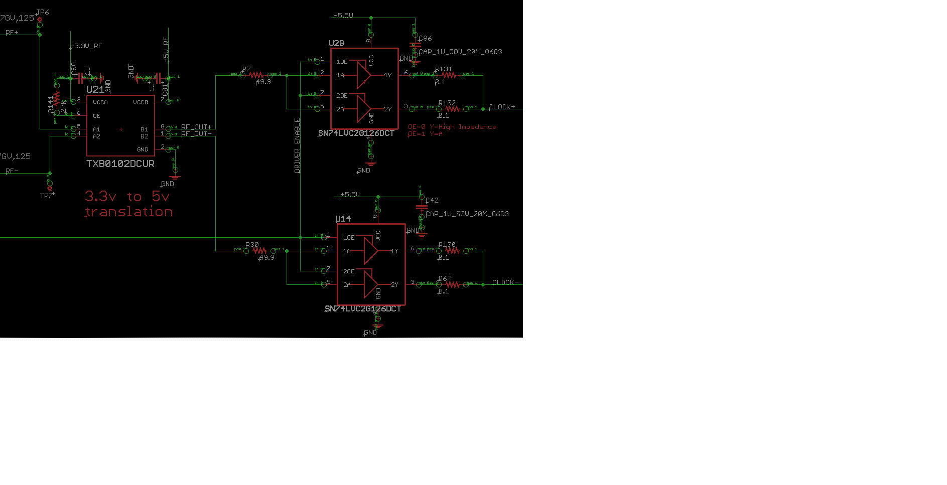
Part Number: TXB0102
Other Parts Discussed in Thread: TXU0102, , SN74LVC2G126
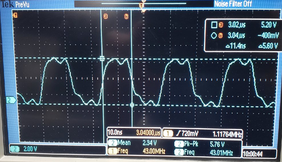
In the attached schematic, I am sending in a 42MHz clock signal.
At TP6 and TP7, the clock signal looks very good. (A nice square wave 0 to 3.3V at 42MHz)
After the TXB0102DCUR level translator, At the left sides of R7 and R30,
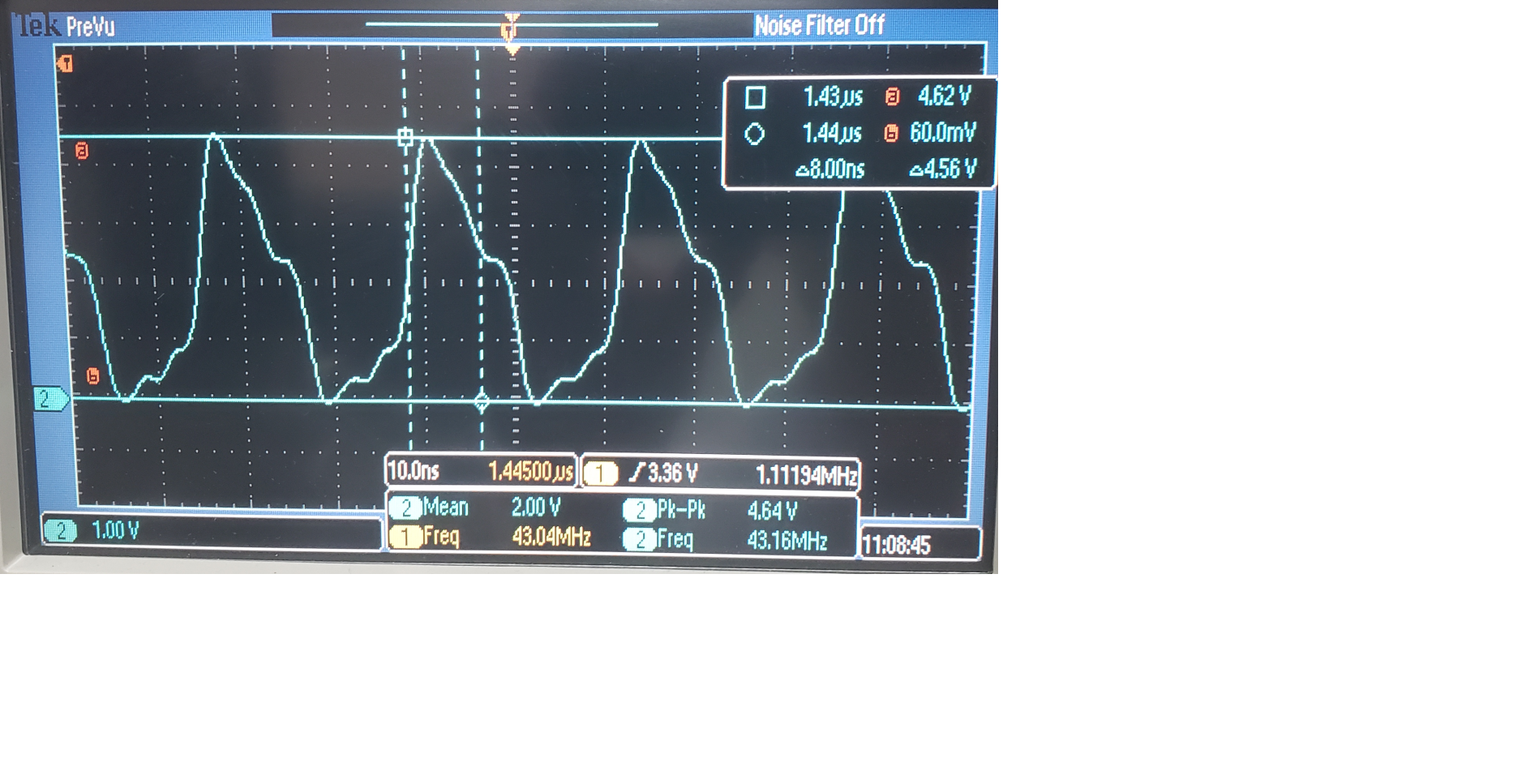
the square wave is very distorted, (as shown in the attach picture of Oscope,
and the clock signals coming out of U29 have a very thin positive duty cycle (about 6ns instead of the expected 11.5ns)
What can I do to fix this.
Note: The +3.3V_RF and +5V_RF signals are also stable, and have < 200mV ripple
 R30
R30