This thread has been locked.

If you have a related question, please click the "Ask a related question" button in the top right corner. The newly created question will be automatically linked to this question.

TXB0106: Series resistance.

Part Number: TXB0106
Other Parts Discussed in Thread: PCA9535, TXU0304, TXU0104, TXU0204

HI 

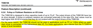
We are using the TXB0106 in unidirectional operation as shown in the document below.

VCCA is 1.8V and VCCB is 3.3V.  The inputs, CELL($)_LT_1V8_VREG, are outputs from 

individual 1.8V LD0's

We have changed the 10K series resistors (R196 through R200)  to 1K  and then to 22 Ohms. 

At 1K the A($) input pins are at 1.65V and at 25Ohms they are at 1.8V.

I though the input load current was in the order of +/-2 uA max. It looks like we have around 

150uA, given that we are dropping 0.15V across a 1K series resistor. 

Am I misreading the datasheet? I also see that there is a requirement for the external drivers to have

drive capability of minimum of +/-2mA , which I assume is driving the gate capacitances and the 

one shot logic on "transitions".  

Is 22 ohm series resistance OK for this application or would you recommend a different value?

Regards

Finbarr

TI_TXB0106.docx

  • Hi Finbar,

    This would typically depend on your type of transmission line. However, I presume you are using a 50 ohm impedance line, hence 22 ohm series resistance is okay.

    You may also see [FAQ] What happens when I connect a logic device's output to a 50 ohm transmission line? for more information.

    Please also note to allow bidirectional transmission, the TXB devices were designed with weak outputs so that other devices can override the device i.e the outputs having a drive strength of only 20 µA. Hence, we typically would not recommend for unidirectional applications where higher drive strength may be required. You may also see TXV0106, thanks.

    Best Regards,

    Michael.

  • HI Michael

    Thanks for the reply. I have a follow up question. would you prefer if I closed this one out and opened a new question?

    Thanks

    Finbarr

    The follow up question is (hopefully not a stupid one):

    If I have a 100K pull down on B1. The B1 input is connected to a device which powers up as high impendence input until it is later configured as an output (hence the use of the pull down. If A1 is connected to a high impedance input with a 100K PU. Will the TXB0106 detect B1 as an input and drive A1 low in the absence of transitions.

    Regards

    Finbarr

  • The TXB does not detect the direction; the output drivers on both sides are always active. (This is why they must be weak.)

    To ensure that channel 1 is low after power up, put pull-downs on both A1 and B1.

  • Wow, interesting. 

    So the pull down on B1 will not guarantee a 0 on A1. I would need to add a 1M pull down on A1 (since there is already a 100K PU on A1) to guarantee a low on the A1 output.

  • Hi 

    Sorry for being so pedantic but we have been seeing some erratic behavior so I just want to double check that what we are doing is now correct before we go to re-layout our PCB 

    With reference to the attached file.

    1) On power up the CELL($)_LT_1V8_VREG signals will transition from 0 to 1 and are driven by separate LDO's. The corresponding outputs LT_COM_CELL($)_VREG are connected to PCA9353. The PCA9535's will initially be powered off and at some time later will be powered up and the ports corresponding to LT_COM_CELL($)_VREG will be configured as inputs. 

    TI_mod_TXB0106.docx

    2) On power up the LT_COM_CELL($)_SIM_DETECT_N signals will not be driven by the PCA9535 (the corresponding ports with be high impedance inputs. WE thought that having R182 through R186 pulled low would be sufficient to have the outputs COM_1V8_CELL($)_SIM_DETECT_N driven low. But form your previous correspondence you do not believe this to be the case. Could you help us understand this better.

    As mentioned before the COM_1V8_CELL($)_SIM_DETECT_N signals are PU to 100K on the modems that they are connected to(we do not have control of these values. So we have added , in line with your suggestion in previous correspondence , a 1.24MOhm PD to ensure that we power up A1 though A5 of U14 low. Vih i s1.26V min and Vil is 0.54V max for the COM_1V8_CELL($)_SIM_DETECT_N signal inputs.

    Can you see any issue with the modified circuitry?

  • Hi Finbar,

    1. Help ensure LDO and PCA are not driving inputs into TXB at the same time. Also note below:

    2. Please help see the datasheet's section 9.2.2 on what to expect. You may also see Effects of PU / PD of TXB further clarifying. For example, table 4 highlights how stronger PD results to lower VOH values out of the TXB device, thanks.

    Best Regards,

    Michael.

  • Thanks Michael

    Just to clarify, from something your colleague Celemins mentioned. On power up , in the absence of transitions on inputs (or outputs) will I need the 1.24M pull downs on the COM_1V8_CELL($)_SIM_DETECT_N signals (they already have 100K PU's on them) , to guarantee that these signals will power up "low". My reading of the situation was that the 100K PD's on the B pins would drive the A pins low, all be it 4k in series with the 100K PU.

    Regards

    Finbarr

  • Hi Finbarr,

    To ensure that channel 1 is low after power up, put pull-downs on both A1 and B1.

    Clemens' feedback is to help ensure a low on the I/O. Note that this is for both A and B sides. Ensuring the input is low also ensures a low output.

    To further clarify, adding 1.24M PD with COM_1V8_CELL($)_SIM_DETECT_N signals having 100K PU's should create a voltage divider of about 1.6V.

    The stronger the PD, the lower the output voltage. For example, 10K PD with 100K PU should output about 0.2V.

    I would not recommend the voltage divider network if you do not intend for the outputs to be always low. Hence, I would further recommend no PD and toggling the OE pin externally instead i.e disabling / enabling the I/Os, thanks.

    Best Regards,

    Michael.

  • HI Michael

    Thanks for your response and sorry for my stupidity (1.24M) PD. I am missing something in my reasoning though. We are only using the device in unidirectional operation. Why is the 100K PD to GND on the B ports not not sufficient to drive the A port low (with 100K PU on the A port and no PD)? Do you need a transition on the B port to drive the A ports high or low? 

    Thanks

    Finbarr

  • As I said above, both directions are always active. If pin A is high and pin B is low, then either pin A overrides pin B, or pin B overrides pin A, and which of the two possibilities happens is random.

    For unidirectional signals, you should use unidirectional translators, e.g., TXU0104/TXU0204/TXU0304.

  • Thanks for all your support

  • Hi Finbarr,

    You are welcome, and all questions are welcomed as we are glad to help, thanks.

    Best Regards,

    Michael.