This thread has been locked.
If you have a related question, please click the "Ask a related question" button in the top right corner. The newly created question will be automatically linked to this question.
Hi,
Please see below queries and request you to suggest
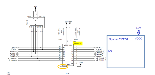
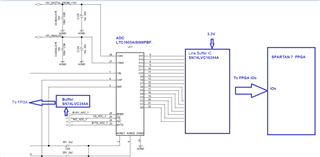
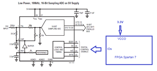
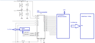
Query1: Regarding 8 Bit Buffer IC SN74LVC244ARGYR , do you have similar one with 16 bit ?
TSSOP package is also fine in 16 bit i.e. Similar to 8 bit SN74LVC244APW
Query 2: Can you please suggest 8 bit bidirectional Buffer ICs whose inputs are tolerant to 5V or above ?
Please reply soon as possible.
Regards,
Puspam Nayak
1. SN74LVC16244A
2. Bidirectional buffers are called transceivers and have the number 74xxx245, e.g., SN74LVC245A.
Thank you Clemens for the information. SN74LVC16244A looks good.
Need to check SN74LVC245A, I was planning to replace below TXB0108PWR with SN74LVC245A however not sure if SN74LVC245A will solve the purpose because B side is 5V and A side is 3.3V
Regards,
Puspam
To convert from 3.3 V to 5 V, you do not need a buffer but a level shifter.
What are the directions of the eight signals? Why don't you want to use the TXB?
Hi Clemens,
Was looking to simplify the design by using Buffer whose inputs are 5V tolerant. In the case of Unidirectional signals usage of SN74LVC16244A is fine (inputs are Vi =5.5V tolerant, Vo= Vcc = 3.3V) however for Bidirectional signals I believe usage of TXB is appropriate.
Regards,
Puspam
To convert unidirectional signals from 3.3 V to 5 V, you could also use a buffer with TTL-compatible inputs, e.g., SN74AHCT244. (This optimizes for price, not for BOM simplicity.)
If you have unidirectional signals in different directions, the best choice would be a combination of TXU translators (TXU0104/TXU0204/TXU0304/TXU0102/TXU0202/TXU0101).
For bidirectional signals (without a direction control signal), you have to use the TXB.
In my design most of the signals are from 5V to 3.3V so planned to go with SN74LVC16244A, SN74LVC244A.
Can you please confirm if selections of these Buffers between ADC LTC1605AISW#PBF and FPGA Spartan 7 is okay? FPGA IOs is configured as LVTTL Inputs
These buffers are OK for the signals output by the ADC (Dxx and /BUSY).
For /CS, R/C, BYTE, you need to translate up. If you want a single chip for all four ADC control signals, the TXU0304 would match; if you have more signals, separate SN74LVC244A and SN74AHCT244 (or similar) would be fine.
Control signals are being driven by FPGA's IO pins, so these control signals are of 3.3V i believe. Referred datasheet of ADC also, below screenshots of ADC datasheet (Part no. LTC1605AISW#PBF)
Wish you very Happy New Year in advance :)
Best Regards,
Puspam Nayak
The /BUSY signal goes in the other direction, so you have 3 and 1 in each direction (when looking only at the four control signals.)
Yes, 'Busy' signal (Unidirectional) going to FPGA input Pin so in my previous block diagram have shown that i will be using. SN74LVC244A i.e. 8-bit buffer between ADC and FPGA. Attaching the screenshot again, check left side of block diagram BUSY. Other 3 i.e. CS, R/C, BYTE will be controlled by FPGA.