This thread has been locked.

If you have a related question, please click the "Ask a related question" button in the top right corner. The newly created question will be automatically linked to this question.

CD74HCT221: pulse width theoritical calc vs measured values dont match at first multivibrator output ?

Part Number: CD74HCT221
Other Parts Discussed in Thread: SN74221, SN74LV221A

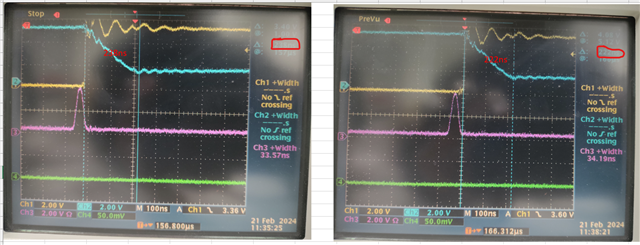
I did replace U1 IC from SN74221NE4 to CD74HCT221, one of the reasons is SN74221NE4 part output signal varies a lot based on the input trigger frequency.

One problem solved specifically related to TP32, which is pretty much consistent with CD74HCT221 part, output signal variations is within 8us at TP32 compared to ~36us variations on previous part SN74221NE4.

Reason for reaching out : at TP27 output, theoretical calc does not match with the measured values (capture below at point 4), atleast want to have kind of justification why it does not match.

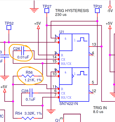
In the following circuit, with R56 = 1.21K ohm and C26 = 0.01uf, pulse width calculations done per 0.7 x R X C.

Considering tolerance of the Resistor and the capacitor, theoretical calculations shown TP27 min, typical and max in bold font herewith

Min 7.64E-06
Typical 8.47E-06
Max 9.34E-06

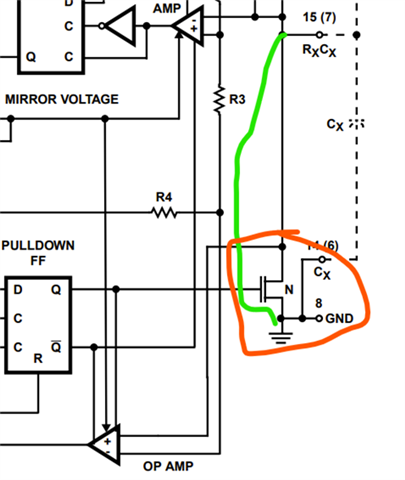
1.) On a bare IC : pin6 and  pin14 CX pins on this IC CD74HCT221 were shorted to ground pin8, this seems expected from the functional diagram, once trigger is received Cext cap discharges via internal MOSFET. 

where as the previous part SN74221NE4 pin6 and  pin14 CX pins does not have short to pin 8 ground.

2.) I am trying to see the output pulse width at TP27 variation based on the components R, C tolerances and also based on IC output tolerance itself

3.) I think CD74HCT221 IC has 2% output tolerance, in my calculations I have considered 7% (based on previous part SN74221NE4 data spec), definitely not logical, but I can update it to 2% based on feedback/comments

R56 1% TOL         Considering tolerances of R and C values  
1210 12.1 1197.9 1222.1     ln2 R56 C26    
            0.7 1.21E+03 1.00E-08 8.47E-06  
C26 2% TOL         0.7 1.20E+03 9.80E-09 8.22E-06  
1.00E-08 2.00E-10 9.8E-09 1.02E-08     0.7 1.22E+03 1.02E-08 8.73E-06  
                     
            Considering tolerance of IC itself  
Min 7.64E-06         7.64E-06   7.88E-06   8.11E-06
Typical 8.47E-06       8.22E-06 5.75E-07 8.47E-06 5.93E-07 8.73E-06 6.11E-07
Max 9.34E-06         8.79E-06   9.06E-06   9.34E-06
                     

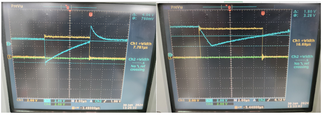
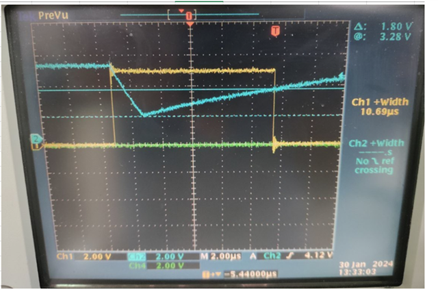
Point 4: Measured width at the output pin at TP27 is 10.69 us?

Overall at TP27 this device CD74HCT221 really consistent in its output pulse width of 10.7us irrespective of trigger frequency(PIN 2) of 1 to 4khz.

point 5 : typical theoretical calc came around 8.4us, which pretty much does match with the charge timing of the capacitor right after the first ~2us of discharge period

How to interpret this behavior as the output timing at TP27 does not match with theoretical calc values? 

In the following as soon as the trigger is received at pin 2, the multivibrator output TP27(Ch1) goes high and the pin15(ch2,blue) scope capture shows it starts discharging, In general the cap should discharge very fast compared to ~2us in this case? any comments about the reason?

In the following screen shot : ch1 is the TP27 and Ch2(blue) is pin 15(Rx/Cx) of IC U1 CD74HCT221 
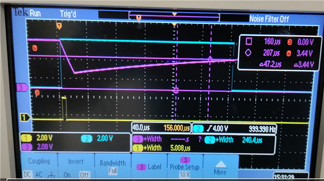
Point 6:

In the following image, I captured for the second section of the multivibrator, 

ch1 is the trigger signal at pin 2

ch2(blue) is the output signal at pin 5,

ch3(purple) is at the pin 7(Rx/Cx)

As this second multivibrator set to 230us, overal pulse width observed is 240us, out of which the discharge time of the capacitor is observed as ~16us.

I did not want to confuse with this extra dataset :-) .  Seems like based on the set RC timings, the discharge time does vary ?

I could not paste the image in this window, attaching it at the end of this request , named as image for point 6. 

Overall at TP32 this device CD74HCT221 really consistent in its output pulse width +/- 8us between trigger frequency of 1 to 4khz.

Min 233us
Max 241us

Image for point 6

  • Hi Vinay,

    How many devices have you tested this on? Only one? 

    I am wondering if this is just a phenomenon observed due to process variations.

    Best,

    Malcolm

  • I tested 5 devices so far, all of them having similar response at TP27 (10.5us to 10.7us).

  • Hi Vinay, 

    To simplify the issue you are seeing is that "real tests" show 10.5 us when "theoretical tests" show 8.4 us? Correct me if I'm wrong here, it's a lot of information, I am just trying to debug this step by step. 

    Most the timings will be based off of the external resistor and capacitors. Have you measured the values of these and checked the tolerance? 

  • Hello Albert, 

    Yes, you are spot on with my question, exactly correct point.

    Value of resistor is 1%(R56) and Cap(C26) is 2%, that's how the theoretical calculations done.

    I did measure those values on board and are within the tolerance spec.

    The difference is the way the trigger discharges the capacitor within the device:

    • On the left is the present part SN74221
    • On the right is the proposed part CD74HCT221

    Theoretical calculations does match with the charge time ramp(as seen in the right side image) of ~8.5us,

    however the excess of ~2 us is due to discharge time duration captured in the right side image.

    My concern is, typically once trigger is received at pin 2, cap should be able to discharge instantly say in the order of 200 or 300ns in general, but it is observed CD74HCT221 part taking ~2us to discharge ? 

    In the following screen shot : ch1 is the TP27 and Ch2(blue) is pin 15(Rx/Cx) of U1 IC

    pls note : left image is for part SN74221, right image is for part CD74HCT221

  • Hi Vinay,

    I forwarded this to another member of our team, I will wait to see if they have any more input on this. 

  • Hi,

    Any update on this query?

  • Hi Vinay,

    First point, someone made a comment on was regarding the 2% tolerance capacitance, is this a typo and should be 20%? As a 2% capacitor is almost unheard of. 

    Regardless, it seems you have specifically measured the real values of the RC components. The good thing is you have technically done all your steps correct. You have already calculated your desired theoretical value, and now after prototyping, you see that is is a bit off. Unfortunately, MMVs are not known to be precise and the difference you are seeing is not surprising. The next step you should look into is to adjust the R value to get the desired pulse width. 

    The summary: 

    MMVs are not precise at all, if you need precision you would most likely have to change to an MCU. However, the difference in timing seen is pretty "normal". You can use all the calculations you have done and adjust R to achieve the final value. 

  • Hello Albert,

    Thank you for the feedback.

    There is no typo error, herewith Cap value used at C26 location is 2% tolerance : BFC241841003 from vishay, CAP, POLYPROPYLENE FILM, .01uF, 250V, 2%, 5mmLS.

    I do not have issue about the consistency of the part CD74HCT221, my observation overall seems really good .  But am trying to understand the basic functionality of this part.

    Overall I see there is an additional discharge time which varies based on R and C values, does not align with the general functionality of discharging within 200 or 300ns  Vs 2us ?

    ~2us to discharge if my R56 and C26 are : 1.21K(1%) and 0.01uf(2%) 

    My concern is, typically once trigger is received at pin 2, cap should be able to discharge instantly say in the order of 200 or 300ns in general, but it is observed CD74HCT221 part taking 2us ?

    If we do not have a technical reason for the additional time and math of it, also am not sure if the given block diagram is correct or not, we may have to discard this part and find an alternative drop in for the part SN74221NE4, we had used this in most of our legacy designs which again has its own consistency issues which i captured in my other query and shared my feedback in that in detail. 

  • Hi Vinay,

    I originally did the math wrong I used 0.1uF instead of 0.01uF. It seems the issue is 2us for 15mA which definitely doesn't not seem correct. 

    1. Have you tested the smaller capacitor on the second channel? It seems the second channel has 0.1uF. 

    2. Have you tested the 0.01uF capacitor just by itself not connected to the system? 

  • Hi Albert,

    For second channel you could refer to following link, I did capture detailed observations:

    SN74221: SN74221NE4 regarding the pulse width related query - Logic forum - Logic - TI E2E support forums

    However I had also observed the discharge time in the second channel as ~19us, R54 and C28 are : 2.1K(1%) and 0.1uf(10%) .

    To reduce any confusions between the channels, i have limited this query to discuss only channel 1 for now.

    channel 1 : 2us to discharge with R56 and C26 are : 1.21K(1%) and 0.01uf(2%) 

    Based on channel 1 and channel 2 discharge time observations, It seems like there is some correlation with the external components with regards to discharge time, but seeing the logic diagram it does not seem it should have any delay.

    Is it possible get feedback from TI team to clarify if there is any logic diagram difference between CD74HCT221 and SN74221NE4 parts ?

    I could not find internal logic diagram in datasheet for the part SN74221NE4, it will be really helpful if you can share it?

    Am not sure if there is any intentional dead time in FET Driver path (internally its the logic gates and the DFF's).

    Reason for a doubt, there is a N channel and P channel FET?

  • Hey Albert, Vinay,

    Looking at the scope shots provided, it appears that the discharge FET is not working as I would expect. Doing some quick math for a constant current discharge of a capacitor:

    i = C dv/dt = 0.01uF * 3.6V / 2us = 18mA

    I would expect that discharge current to be much larger.

    @Albert,

    Can you get some samples and verify that we see the same issue here in our lab?

    @Vinay,

    I would recommend that you get some of the SN74LV221A device and test in your application - it is the newest of the MMV devices and has the best linearity.

    Is it possible get feedback from TI team to clarify if there is any logic diagram difference between CD74HCT221 and SN74221NE4 parts ?

    I could not find internal logic diagram in datasheet for the part SN74221NE4, it will be really helpful if you can share it?

    Yes, these are quite different from the internal logic perspective. As I mentioned previously, SN74221 is one of the oldest devices we support (around 60 years) and is based on TTL circuitry. The HCT family is newer, but still quite old (closer to 40 years).

    No, we cannot share internal designs of our devices. FYI - the schematics provided in our logic datasheets are only functionally equivalent to our devices. They will not give you a transistor-level design of any device.

  • Hi Emrys,

    Related to your last response:

    SN74221NE4 is a PDIP 16 pin device Vs SN74LV221A SOIC.

    The suggested part SN74LV221A but this calls for a design change(PWA), as I was actually looking for a drop in.

    Also SN74LV221A parts seems have a different truth table as one of the input is negative-transition-triggered, even if we update our HW I doubt if it could work without change in the firmware?

    Pls note, while i checked SN74LV221A datasheet, I see even this part has a discharge window as shown in the following snap, however the overall width looks to be within the expected pulse width (discharge and charge time both inclusive).  Which i believe should have been the same with CD74HCT221 

    All am interested to understand is : once trigger is received at pin 2, cap should be able to discharge instantly ?


    Pls note, I have ordered CD74HCT221 part twice (batch of 5 and batch of 10),

    1.) all of them had the extra 2us period only on channel 1, 8.5 us configured time => ~10.5us

    discharge time + charge time was not matching set pulse width

    R56 and C26 are : 1.21K(1%) and 0.01uf(2%) 

    2.) whereas channel 2 was very consistent to provide configured time which includes the discharge time 

    discharge time + charge time was matching to set pulse width

    R54 and C28 are : 2.1K(1%) and 0.1uf(10%)CD74HCT221E.zip

    In channel 2: all of them had discharge time of ~19us period, however overall pulse width (discharge time + charge time) was very consistent to the set pulse width.

    => am sure you had seen and replied to my past observations in the following link.

    SN74221: SN74221NE4 regarding the pulse width related query - Logic forum - Logic - TI E2E support forums

    Am also attaching the captured images for 10 sets of CD series parts ordered as second batch - bear with me on file size (180MB)

  • Hi Vinay,

    Thanks for the detailed scope captures. And explanation of why the LV-A part won't work for you at this time.

    All am interested to understand is : once trigger is received at pin 2, cap should be able to discharge instantly ?

    It is not possible for a capacitor to instantly discharge, but I expect you mean to say, "should the cap be able to discharge faster?"

    I'm afraid I don't know that answer for this device due to its age and origin (built/designed by Harris, acquired by TI). I don't have a design file to refer to, so I can't even check the relative FET sizes.

    It appears to me that the device is operating consistently; it is just not 100% aligned with the typical characteristics plots in the datasheet. The datasheet is on our list to update in the next two years.

    My usual recommendation for using a monostable multivibrator is to:

    1. Estimate required RC values using the datasheet plots

    2. Build a prototype using the planned resistor and capacitor components and test the output pulse width (across temperature, if possible). Calculate K from the tested components. K = tw / (R * C)

    3. Recalculate R and adjust R value to get the required pulse width, keeping in mind that these are not precision instruments (expect up to 10% variation in the worst case from process / temp variations)

    4. Re-test with adjusted R value to ensure the pulse width falls within system requirements.

  • Hi Albert,

    Did you get a chance to run the tests?

    Did you see similar observations as I do?

    Hi Emrys,

    sounds like for any given R, C value manufacturer expects to derive K, unless we go with what was suggested by the manufacturer.

    This will be a one time effort when designer’s change those values. 

    May be this has to be clearly captured in your datasheets to make sure everyone understands and be on same page.

    K value is calculated based on onboard measurements

    R56

    1% TOL


    TP27

    Considering tolerance of IC itself(7% instead of 10%)


    1210

    12.1

    1197.9

    1222.1

    Min

    9.95E-06

    ln2

    R56

    C26


    9.95E-06


    Typical

    1.07E-05

    8.84E-01

    1.21E+03

    1.00E-08

    1.07E-05

    7.49E-07

    C26

    2% TOL


    Max

    1.14E-05


    1.14E-05

    1.00E-08

    2.00E-10

    9.8E-09

    1.02E-08

    Diff

    1.50E-06


    R54

    1% TOL


    TP32

    Considering tolerance of IC itself(7% instead of 10%)


    2100

    21

    2079

    2121

    Min

    1.43E-04

    ln2

    R54

    C28


    1.43E-04


    Typical

    1.54E-04

    7.32E-01

    2.10E+03

    1.00E-07

    1.54E-04

    1.08E-05

    C28

    10% TOL


    Max

    1.64E-04


    1.64E-04

    1.00E-07

    1.00E-08

    0.00000009

    0.00000011

    Diff

    2.15E-05


  • Hi Vinay,

    Today is currently a holiday. However, the samples I ordered have still not come in (should be this week). I will look to conducts these tests ASAP. 

  • Hello Albert/Emrys,

    I was trying to some more checks, while I see in one channel we had 0.01uF cap(C26) and other channel we had 0.1uf(C28).

    we see ~2us discharge time with channel having 0.01uf Vs we see ~20us discharge time with channel having 0.1uf(C28), which makes me to figure out what would be effect by further reducing the cap value.

    C

    discharge time
    0.001 uf 0.22us
    0.01 uf 2us
    0.1 uf 20us

    So I did give a try to replace both C28 from 0.1uf to 1nf and C26 from 0.01uf to 1nf.

    Ofcourse updated the resistance values too.

    Both locations, I could see the discharge time reduced to ~ 220ns or 0.22us.  Which does confirm the discharge time is purely based on the external cap value.  sounds like I got my answer for which i raised this discussion for.  Appreciate if you can review and comment on.

    *Following checks were done on a bench test set up on a breadboard with CD74HCT221.

    In the following CH1(Yellow/Orange) is the unstable state output, CH2(BLUE) is at CXRX pin(discharge time), CH3 is the external trigger signal.

    *pls discard the pulse width of CH3(purple) in this image, overall response does not change anyway with higher pulse width till 5us.

    By mistake I went down to that width, but I did retest for our use case of 5us pulse width at CH3(external trigger).

    Left hand side captured image is at channel 1 output 

    Right hand side captured image is at channel 2 output


    But am having issue on the K factor value.

    I did try to recalculate K factor based on test checks, but my channel 2 output TP32 is not consistent enough at 6Khz trigger rate.

    Also let me know if its fine to use higher value of resistance, I could not see what's the max value of R that can be used.

    In Channle 2, with higher R value(210K) I could not get a better response/consistent value with 6Khz trigger

      K R C Tw Test point Trigger freq
    CH1 8.26E-01 12100 1.00E-09 1.00E-05 TP27  
    CH2 7.76E-01 210000 1.00E-09 1.63E-04 TP32 6.13E+03

    I updated the channel 2, R value 21.5K and and C to 0.01uf to meet 7khz trigger at CH2, this was giving very consistent output of 140us.

    It sounds like CD74HCT221 part has limit on the resistor that can be used, following set R, C values give me consistent output for both CH1 and CH2.

      K R C Tw Test point Trigger freq
    CH1 8.26E-01 12100 1.00E-09 1.00E-05 TP27  
    CH2 6.51E-01 21500 1.00E-08 1.40E-04 TP32 7.14E+03

    Appreciate if you have any comments or feedback, that will be really helpful.

  • Hello Albert/Emrys,

    Any comments or updates, based on your inhouse test checks/discussions or based on my last message observations?

  • Hey Vinay,

    we see ~2us discharge time with channel having 0.01uf Vs we see ~20us discharge time with channel having 0.1uf(C28), which makes me to figure out what would be effect by further reducing the cap value.

    That is what I would expect -- when discharging the capacitor, the internal FET is put into saturation and thus has a constant current discharge. 10x capacitor = 10x time to discharge.

    I did try to recalculate K factor based on test checks, but my channel 2 output TP32 is not consistent enough at 6Khz trigger rate.

    It looks to me like you calculated the K factor just fine -- recall what Albert mentioned earlier:

    MMVs are not precise at all, if you need precision you would most likely have to change to an MCU. However, the difference in timing seen is pretty "normal". You can use all the calculations you have done and adjust R to achieve the final value. 

    I would not expect better than 50% accuracy with an MMV + external RC. Even with an amazingly accurate capacitor, I'd still not give it better than 10% accuracy.

    Also let me know if its fine to use higher value of resistance, I could not see what's the max value of R that can be used.

    Usually the resistance limit is based on leakage current - ie at some point your resistor is so large that even small leakage currents will cause voltage shifts. See the EC table in the DS for leakage current values, and use Ohm's law for the voltage drop across the resistor. I would recommend never exceeding 500kohm with an MMV, and generally it's good to stay between 10k and 100k.

  • Hi,

    Evaluated to recheck with different ordered samples, with following set of values, got very consistent results.

    us us us us us us
    Digikey Order1 CD74HCT221E   Min 133 Max 136 Diff 3     Min 9.6 Max 10 Diff 0.4  
      CH2(TP32), C28=0.01uf, R54=19.6K ohm CH1(TP27), C26=0.001uf, R56=12.1K ohm
    Sample# Pulse(1sec) 1Khz 2Khz 3Khz 4Khz 5Khz 6Khz 7Khz 8Khz Pulse(1sec) 1Khz 2Khz 3Khz 4Khz 5Khz 6Khz 7Khz 8Khz
    D1 135 135 134 135 134 134 134 134 134 9.8 9.7 9.9 9.9 9.8 9.8 9.7 9.6 9.8
    D2 135 134 134 134 134 134 134 134 134 9.7 9.9 9.9 10 9.9 9.8 9.8 9.8 9.7
    D3 135 135 134 135 134 135 134 134 135 9.8 9.8 9.9 9.9 9.9 9.9 9.8 9.7 9.9
    D4 135 135 133 134 135 135 135 134 135 9.8 9.8 10 10 9.8 9.9 9.8 9.9 9.9
    D5 134 133 134 134 134 134 134 133 134 9.9 9.9 9.9 9.9 10 9.8 9.8 9.8 9.9
    D6 135 134 134 134 134 135 134 134 134 9.6 9.8 9.8 9.9 9.8 9.9 9.6 9.6 9.8
    D7 135 135 135 135 135 135 134 135 135 9.8 9.8 9.8 9.8 9.9 9.8 9.8 9.7 9.8
    D8 136 136 136 136 136 136 136 136 136 9.9 9.9 9.9 9.9 9.9 9.9 9.8 9.8 9.9
    D9 136 136 136 136 135 136 136 136 136 9.8 9.9 10 9.9 9.8 10 10 9.8 9.8
    D10 135 135 135 135 135 135 135 134 135 9.9 9.8 9.8 9.8 9.9 9.8 9.7 9.7 9.8
                                         
            us us us     us us us  
    Mouser Order2 CD74HCT221E   Min 133 Max 135 Diff 2     Min 9.4 Max 9.8 Diff 0.4  
      CH2(TP32), C28=0.01uf, R54=19.6K ohm CH1(TP27), C26=0.001uf, R56=12.1K ohm
    Sample# Pulse(1sec) 1Khz 2Khz 3Khz 4Khz 5Khz 6Khz 7Khz 8Khz Pulse(1sec) 1Khz 2Khz 3Khz 4Khz 5Khz 6Khz 7Khz 8Khz
    M1 134 134 134 135 134 134 134 134 134 9.7 9.6 9.6 9.7 9.7 9.5 9.5 9.6 9.6
    M2 135 134 135 134 134 134 134 133 133 9.8 9.8 9.8 9.6 9.8 9.8 9.6 9.6 9.7
    M3 134 134 134 134 133 134 134 133 134 9.6 9.7 9.6 9.6 9.6 9.5 9.5 9.5 9.7
    M4 134 134 133 134 133 134 134 133 133 9.7 9.7 9.7 9.7 9.7 9.6 9.5 9.5 9.8
    M5 134 133 133 133 134 133 133 133 133 9.8 9.8 9.8 9.8 9.8 9.8 9.6 9.7 9.7
    M6 134 134 134 133 133 134 133 133 134 9.8 9.8 9.8 9.8 9.8 9.8 9.6 9.6 9.8
    M7 135 135 135 134 135 134 134 133 135 9.7 9.7 9.7 9.7 9.6 9.6 9.6 9.5 9.7
    M8 135 134 134 135 135 135 134 134 135 9.6 9.7 9.6 9.7 9.7 9.7 9.5 9.6 9.7
    M9 134 134 134 133 134 134 134 133 134 9.7 9.5 9.5 9.6 9.7 9.6 9.5 9.4 9.7
    M10 134 134 133 134 133 133 134 133 134 9.7 9.7 9.7 9.7 9.6 9.7 9.6 9.5 9.7
    us us us us us us
    Mouser Order3 CD74HCT221E   Min 132 Max 135 Diff 3     Min 9.3 Max 9.9 Diff 0.6  
      CH2(TP32), C28=0.01uf, R54=19.6K ohm CH1(TP27), C26=0.001uf, R56=12.1K ohm
    Sample# Pulse(1sec) 1Khz 2Khz 3Khz 4Khz 5Khz 6Khz 7Khz 8Khz Pulse(1sec) 1Khz 2Khz 3Khz 4Khz 5Khz 6Khz 7Khz 8Khz
    M1 134 134 134 134 133 134 133 134 134 9.6 9.6 9.6 9.5 9.5 9.6 9.5 9.4 9.6
    M2 134 134 133 134 134 134 134 133 134 9.6 9.7 9.7 9.6 9.7 9.6 9.4 9.5 9.6
    M3 135 135 135 135 135 135 134 135 135 9.7 9.6 9.7 9.7 9.7 9.7 9.5 9.6 9.6
    M4 134 134 134 134 134 134 133 134 134 9.8 9.9 9.9 9.9 9.9 9.8 9.7 9.6 9.8
    M5 134 134 134 133 134 134 133 132 133 9.9 9.8 9.8 9.9 9.9 9.8 9.8 9.8 9.9
    M6 133 132 132 133 133 132 132 132 131 9.9 9.8 9.8 9.8 9.8 9.8 9.8 9.8 9.8
    M7 134 134 134 134 134 134 134 133 134 9.8 9.8 9.7 9.7 9.8 9.7 9.6 9.5 9.8
    M8 134 134 134 134 134 134 134 134 134 9.7 9.6 9.6 9.6 9.7 9.7 9.6 9.5 9.7
    M9 134 133 134 134 134 132 134 133 133 9.6 9.6 9.6 9.6 9.7 9.6 9.5 9.5 9.6
    M10 134 134 134 135 135 135 135 134 134 9.5 9.4 9.5 9.3 9.6 9.5 9.3 9.3 9.5
  • Hey Vinay,
    I'm glad to see that your testing has been very consistent.

    I would just like to remind you that these are likely all devices coming from the same lot of material, and you can still see shifts when doing mass production. Please don't count on this type of device for precision timing without adding some type of check in your production flow.

  • Yes I agree Emrys,

    I just shared as reference and at times it might helps others too.

    Meanwhile I have planned to have some tolerance captured in the test spec.

    Really helpful discussion, thank you(Emrys & Albert) for your patience in reviewing and providing feedback.