This thread has been locked.

If you have a related question, please click the "Ask a related question" button in the top right corner. The newly created question will be automatically linked to this question.

LSF0102: LSF0102 internal MOSFET architecture

Part Number: LSF0102

Hi experts,

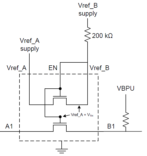
Want to know the internal MOSFET architecture about LSF family. From training video said it is a four pin MOS, and from the illustration, base side connect to GND and Gate connect to Vbias.

1.Can you provide details of the internal MOSFET connect, construction and work status? The video is not very clear.

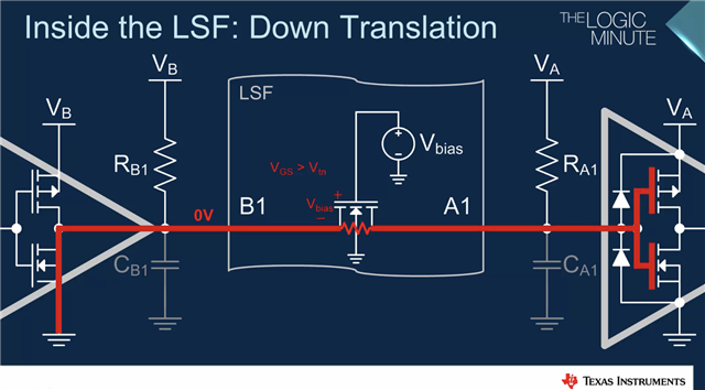
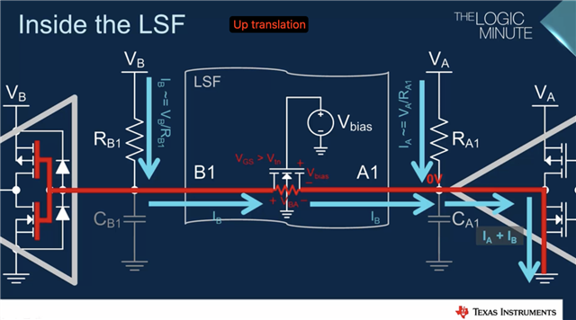
2.From data sheet and training video there is no transition waveform of DownStream(B drive A). Can you provide both Up/Down waveform? Due to LSF family is bi-direction LS, if the pass FET is connected as 3 pin NMOSFET, the transitions of UpStream and DownStream should be different.

Thanks

  • See the LSF application report.

    1. They are plain N-channel MOSFETs (with the body connected to GND). What exactly do you want to know?

    2. The MOSFETs are symmetrical; it does not matter which side you call source or drain. All voltages are clamped at Vref_A; any higher output voltage must be generated by pull-up resistors. You can put pull-up resistors on any I/O pin, and the pull-up voltage can be different at any pin (but must not be smaller than Vref_A).
    When translating from a higher to a lower voltage, the output voltage follows the input voltage, but is clamped at Vref_A. If the output pin has a pull-up, the output voltage does not go below that voltage.

  • The MOSFETs are symmetrical; it does not matter which side you call source or drain. All voltages are clamped at Vref_A;

    Enhence N-MOSFET turn on by the channel between two n+ node. The electric field on Gate and P-substrate is important to generate and maintain the channel. Turn on condition for N-MOSFET is Vgs>Vth, the reason is the 3 terminal MOSFET will connect body to one of the two n+ node, and the connected one is called Source. My understanding is if body is connect to GND, a small voltage larger than Vth on Gate will turn on the FET. In video Vgs alternate between two node. It does matter where the source/drain is, it will impact the behavior Down or Up translation H2L or L2H.

  • The body is not shorted to either end of the channel. For practical purposes, you can take the A or B pin that is pulled low by the external device and call it "source".

    The gate voltage (= EN) is Vref_A + Vth, so the transistor will turn on when the voltage (on either side) is Vref_A or lower.

  • Hey Allen,

    Clemens' is correct here- the body of the NFET is tied to GND and neither the source or drain, where source/ drain are interchangeable (whichever side is driving the line low can be considered the source). The Vbias circuitry here is refencing to the NFET that connects VREFA & VREFB in order to regulate the gate voltage to VREFA + VTH to all the I/O channel FETs. 

    Understanding the Bias Circuit for the LSF Family

    Regards,

    Jack