This thread has been locked.

If you have a related question, please click the "Ask a related question" button in the top right corner. The newly created question will be automatically linked to this question.

I2C2 acknowledgement and noise issue in camera interface with omap3530

Other Parts Discussed in Thread: TXS0104E, OMAP3530, PCA9306

Hi,

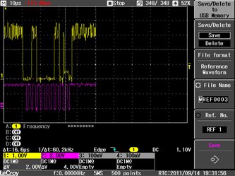
     We use Camera device OV7725 as I2C2 device to interface with the I2C2 host OMAP3530. We use the buffer TXS0104E for level translation between host and device (supporting I2C translation). But here the device is not getting detected both in software and hardware testing. In hardware when we probe the I2C2 data signal, the acknowledgement bit is not going absolute zero, instead stays at some voltage level( around 0.75V). Also there is lots of noise appearing in the signal levels. Please let us know how can we overcome from this issue.

Regards,

Vijetha

  • Hi Vijetha,

    Do you have any external pull-up resistors on the bus? These can cause the LOW output voltage to be higher than 0.4V. If you have any waveforms available, or a schematic showing everything connected to the I2C lines, please share. They will help us debug. 

    The noise from the signal levels may be caused by multiple issues. Do you have bypass capacitors on the TXS0104E? Are the traces close to any noise sources?

  • Hi Hattie,

    Thanks for the reply. Yes, we do have a pull-up resistors of value 4.7K on the device side and processor side. Along with this we also have internal pull-ups of 10K for every pins of the translator TXS0104E. 

    Now we changed the translator for I2C2 lines, i.e we used an I2C translator PCA9306 instead of TXS0104E. For that translator we used 220E pull up at the device side as recommended in datasheet. Still the acknowledgement bit is not going low. We often tried different pull-up resistor values (up to 10K ohm) at the device side. 

    We have bypass capacitors(0.1uF) for the power supplies of the translator.


    The waveform we got when probed at I2C2(data and clock) line near the device is given above. The 9th bit is acknowledgement bit (which is to be zero) appears to be around 0.7V with a spike at the beginning.


  • A spike on the ACK bit can be normal. Sometimes there is a small delay between when the master releases the SDA line and when the slave device pulls it low again for the ACK. This delay will cause the glitch you see. In I2C protocol, the logic level on the SDA line is read on the rising edge of the CLK, so as long as the signal is low before the CLK rises - no communication errors.

    Also, the ACK bit will be at a slightly higher voltage than the other 'LOW,' in most cases should not cause any system level errors. Translators will have a small amount of on resistance. The current driving through the on resistance of the translator will cause the voltage to rise slightly. The best way to lower the voltage is to select the largest pull-up resistor possible, this results in the lowest possible current through the device. 220E? Please send me a schematic so I can provide more advice based on your system.

    I do not know why the signal is so noisy. Have you probed the VCC rail for noise? is the device near any noise sources - like antenna? 

  • I had similar problem and found a cause for my case.

    When both port (A and B) were driven by other devices, this kind of waveform is observed.

    Please check possible driver devices and their output enable control logic.

  • The problem was tracked. I2C2 lines from the processor on main board goes to an I2C2 buffer PCA9306DCUR which drives an IC and a connector. The same I2C2 lines from the processor goes to my daughter board in which also there is same buffer used for 1.8V to 3.3V translation. When the buffer on the main board is removed or when the input/output pins of the buffer on main board are removed, the device on the daughter board is responding with acknowledgement. So the parallel connection of 2 buffers is doubted to be the issue.  In the software it is configured as the I2C goes to buffer on main board 1st and then to daughter board.

    Please suggest me what exactly avoiding device to respond. Is the buffer on daughter board back-driven by another buffer?