This thread has been locked.

If you have a related question, please click the "Ask a related question" button in the top right corner. The newly created question will be automatically linked to this question.

SN74GTL2014: 仿真相关问题——仿真与实测结果拟合不上

Part Number: SN74GTL2014

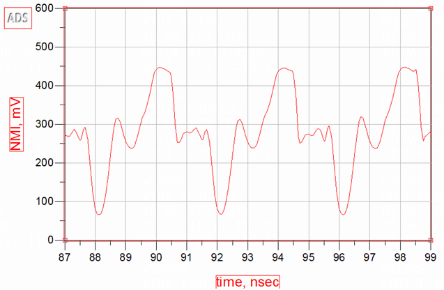
Phenomenon: When using material GTL2014, signal quality issues and reflections were found, which could not be resolved by adjusting the termination resistors. We tried to fit the simulation results, but they did not match the actual measurements and showed significant differences. Therefore, we suspect that there may be something wrong with the simulation.

Question 1: Is it reasonable to use the IBIS model of the 2014 chip as output and the CPU's BUFFER Type as input in the current simulation approach?

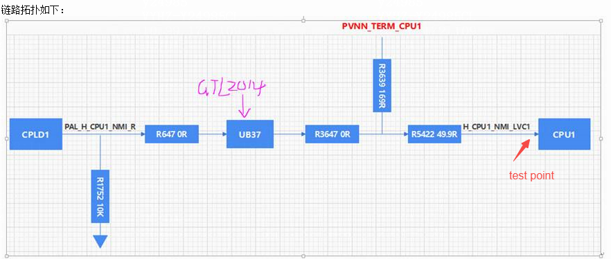
Question 2: Should we also include the relevant links of CPLD1 in the simulation? (Previously thought GTL2014 was isolated, so it was not included)

Question 3: Are there equivalent parameter models for the chip?

Remarks:

1. The signal is a voltage signal.

2. The wiring and parameters of vias in the link are considered.

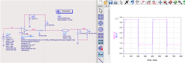
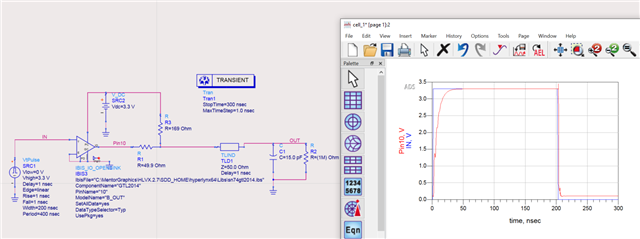
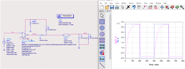
Topology is as follows:

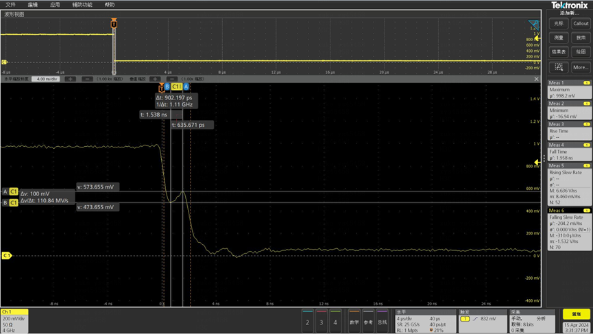
The actual waveform is as follows:

Simulation results:

  • Hi Zhiyuan,

    1. Yes. 
    2. I am unsure the links you mention. As long as the GTL device receives input correctly, it would be okay. 
    3. All other similar GTL devices are relevant. 

    However, please note that the actual waveform step is most likely due to transmission line effects as it seems impedances are actually not matched. 

    Furthermore, I suspect the simulation is actually reading the direct output of the GTL device with all connections instead of the final output of the line at the end of the transmission line (see below), thanks. 

    Similar to your schematic:

    Similar to your first waveform:

    With higher pull-up:

    Best Regards,

    Michael.