This thread has been locked.

If you have a related question, please click the "Ask a related question" button in the top right corner. The newly created question will be automatically linked to this question.

CD4050B: CD4050B Supplementary Q's

Part Number: CD4050B
Other Parts Discussed in Thread: TLV1811, TLV7211, UCC27527

Hi Clemens 

Thanks for your prompt support in the past.

I've a few supplementary Q's, answers to which I could not gather from the Data Sheets.

Pl be good enough to reply at your convenience:

1) Configure it as a Schmitt Trigger ( Need a Positive Logic Schmitt Trigger unlike CD40106 )

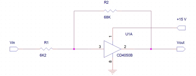
Datasheet Shows Transition ( typ ) @7.5V ,& Vth+ As 11v max , Vth-  as 4V Min . Should I Expect the Following?

Thresholds Rising Edge :   8.2 V Typ, 12 V Max

                   Falling Edge : Min 3.0 V , Typ 6.8 V

2) If i give a Triangular wave of 0V -15V- 0V at the input , What would be the Max Input Current @ transition point 

    Also, if a +15V Input appears when CD4050 is not powered, is the IC safe 

3) Short pulse suppression circuit ( 1 uS Typ )

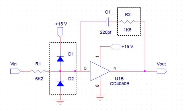
 Do I need R2 (Current limiting at transition point ) & Clamping Diodes D1 &D2 . Max Freq. Is under 20 KHz.

4) Driving a 1nf Capacitor @ 20 kHz Max. Can I Use this:

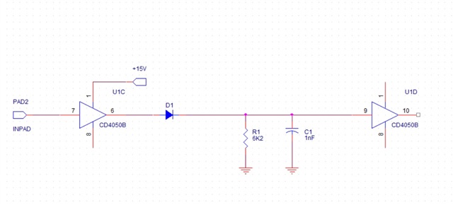
Is CD4050B O/p capable of repeatedly charging 1nF at a Freq  not exceeding 20 KHz 

Thanking you in advance

BR

Varun

  • 1. Yes; this circuit moves the switching thresholds by about 10 %.

    2. The maximum is not specified. It is not expected that you would use slow edges. Also, applying voltages above the supply can violate the IIK absolute maximum rating.

    3./4. You have to ensure that the output current is small enough so that the power dissipation does not become too large.

    I do not know what the actual problem is you're trying to solve, but I think a comparator (e.g., TLV7211 or TLV1811) would work better.

  • Clemens 

    I admire you as my Guru_ji for your knowledge & for your prompt replies.

    Thanks for your answers.

    To reply to your last comment, some of these are for our IGBT Driver Ckts.

    Input is 0-15 V Signals , with reasonably good rise & Fall times , but since 

    they would come from the client's side, their dt/dv may not be guaranteed.

    Schmitt Trigger action preferred and additionally Dead Band Generation 

    of between 2 to 4.5 uS , Interlock and Short Pulse Suppression of approx 1 uS.

    Most Dead Band generating IC's limit to 500 nS, and Short Pulse Suppression

    is almost invariably absent.

    Essentially, Pulses shorter than say 1 uS must be killed , whether for On or Off

    from going over to the IGBT Gates.

    I had a good Ckt with 3 units of UCC27527, now trying to rationalize the same.

    Now I would need one CD4050B, use four gates from that, two for the Input stage

    and two for the SPS , while I would use that UCC27527 for the Interlock and 

    Dead Band generation, using it's CMOS Input for the Dead Band timing;

    effectively saving two nos of UCC27527 and some Real estate on the PCB 

    Thanks again for your very prompt, & in-depth replies, as always.

    Warm regards

    Varun