This thread has been locked.

If you have a related question, please click the "Ask a related question" button in the top right corner. The newly created question will be automatically linked to this question.

SN74AVCH8T245: Transition Timing

Part Number: SN74AVCH8T245

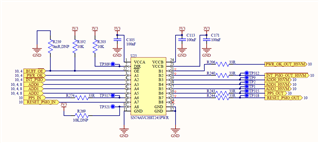
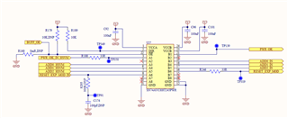
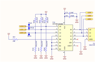
Hi Currently we are using SN74AVCH8T245 8-Bit Dual-Supply Bus Transceiver which has 3.3V RAIL to both VCCA & VCCB and the output being feed to Adder ( CD74HC283M96 ),

Our requirement is using the Bus transceiver the output bit address is 100 and feeding this input to adder P/N mentioned above and expected output to be 101 and following output signal been feed to controller.

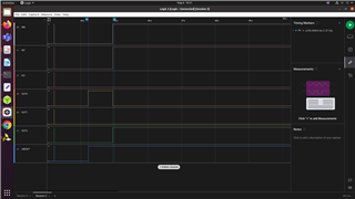
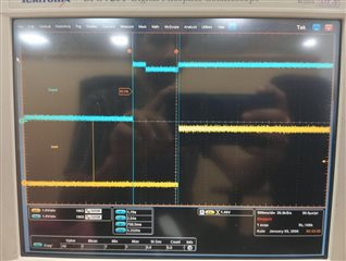
But we are facing an Issue in the inconsistency in the adder output, and not being able to identify where is the issue being caused, Currently we resolved this issue through firmware code by adding 1Sec delay and observed consistency all the time, 

I really would like to know if it has to anything with the hardware or where is it going wrong I am attaching the below images of the circuitry.

Please let me know if any further input required,

Thanks.


  • Please show an oscilloscope trace when the output begins to have a wrong value, and the corresponding input.

  • Hello Dangeti,

    As Clemens mentioned, it will helps us if you share oscilloscope waveforms of the inputs and outputs of the adder.

    Question: Is there a set timeframe the controller needs to receive the 101 value? You said adding a 1 second delay solved the issue, my guess is the propagation delay on the adder is causing inconsistencies. On the AVCH8T the max propagation delay at 3.3V is 2.8ns which isn't much. But on the CD74 max prop delay is 63ns at 4.5V. 

    So by adding a 1 second delay, you give the CD74 time to send all the correct outputs to the controller.

    Regards,

    Josh

  • Hi Joshua,

    As you mentioned here is the result of probing,

    IN0 -----> Adder input signal on ADD0_IN coming from the BUS

    IN1 -----> Adder input signal on ADD1_IN coming from the BUS

    IN2 -----> Adder input signal on ADD0_IN coming from the BUS

    OUT 0 -> Adder output signal ADD0

    OUT1  -> Adder output signal ADD1

    OUT 2 -> Adder output signal ADD2

    nReset -> STM controller boot up time

    From the probing we could see the delay in the output of BUS, because ADDER output is up and proper by the time STM is booting up,

    Regards,

    Ravi.

  • Hi Joshua,

    As you mentioned here is the result of probing,

    IN0 -----> Adder input signal on ADD0_IN coming from the BUS

    IN1 -----> Adder input signal on ADD1_IN coming from the BUS

    IN2 -----> Adder input signal on ADD0_IN coming from the BUS

    OUT 0 -> Adder output signal ADD0

    OUT1  -> Adder output signal ADD1

    OUT 2 -> Adder output signal ADD2

    nReset -> STM controller boot up time

    From the probing we could see the delay in the output of BUS, because ADDER output is up and proper by the time STM is booting up,

    Regards,

    Ravi.

  • The adder appears to work correctly.

    Please show the inputs and outputs of the '245. (An oscilloscope would help to detect invalid logic-level voltages.)

  • Here is the AVC input and output waveform and as we could see there is a propagation delay of 750ms

    and below i have attached the schematic of AVC, can you help me to understand what could be causing this delay.

  • What makes the input signal drop for 500 ms? What happens at the end?