


Hello:
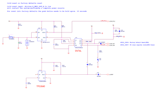
Please assist in conducting a review of the MC project schematic about SN74LVC1G74
Due to the urgency of the project, we hope to receive feedback as soon as possible. Thanks!!!
Hello:
Please assist in conducting a review of the MC project schematic about SN74LVC1G74
Due to the urgency of the project, we hope to receive feedback as soon as possible. Thanks!!!

