A related question is a question created from another question. When the related question is created, it will be automatically linked to the original question.
If you have a related question, please click the "Ask a related question" button in the top right corner. The newly created question will be automatically linked to this question.
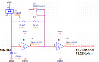
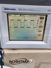
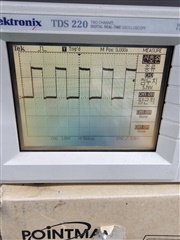
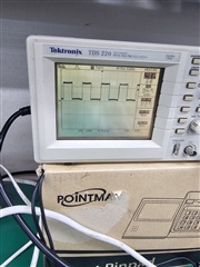
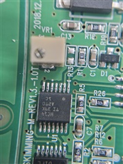
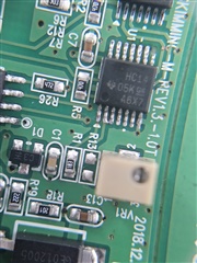
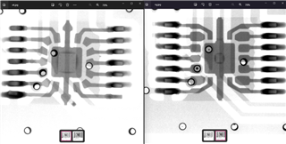
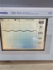
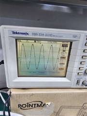
Yes, this device underwent a die revision. Can you show pin 1? If you are discharging/recharging the capacitor for oscillation like Clemens said I wouldn't expect to see a square wave at the input to the inverter.
This is exactly what I would expect to see. And in the question, you said that changing the period is what you wanted to achieve; is the problem solved now?