This thread has been locked.

If you have a related question, please click the "Ask a related question" button in the top right corner. The newly created question will be automatically linked to this question.

LSF0204:A question about LSF family

Part Number: LSF0204

Tool/software:

In this video 2:39, For example,I don't understand the reference in the video

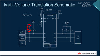
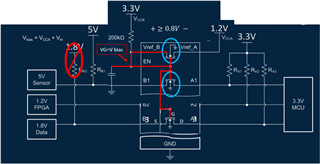
 “on the 1.8-volt data line, if the resistor RB3 were removed, any data sent from the MCU would be translated down to 1.2 volts instead of 1.8 volts.

Where does 1.2V comes from?VccA?

https://www.ti.com/video/series/understanding-the-lsf-family-of-bidirectional--multi-voltage-lev.html#transcript-tab

  • Output voltages are weakly clamped at Vref_A.

  • Thanks for your answer,but i still don't know the process Vref_A affect 1.8V Data line when MCU send high or low .

    in my understanding,when MCU send high,FET will open until VGS <Tn,but 1.8V Data side without pull up RES,how does Vref_A affect 1.8V data line

  • This is explained in the videos "Understanding the Bias Circuit for the LSF Family" and "Down Translation with the LSF Family".

  • Hi Echo, 

    When MCU drives high, VGS (VG= 1.8V, VS = 1.2V) <= VTH. Internal switch will be operating near cutoff region, so the voltage is clamped at A-side voltage. The output side can only be pulled up higher to 1.8V if an external pullup resistor is used. 

    Regards,

    Jack 

  • Thanks Jack,

    I have the following questions

    1:VG=Vbias=VccA+Vth is that right?(as red line show)1.8V=1.2+0.6,

    but i didn't see anything in the video about the Vth is 0.6V.

    2:and VS=1.2V just the VS voltag of the first FET , is that right?

    A3 port and B3 port  which side is the source and which is drain?

    in my understanding,A3 port provide 3.3V to B3, until VGS ≤ Vth FET cutoff,and then i don't know where does B3 port voltage come from,how much it is?

    3:the first FET is always in steady state?

    can it affect channel 3?

    Forgive me for asking so many questions XD.

  • Hi Echo,

    1. Vth can be estimated to be about 0.6V to 0.8V.

    2. Both sides are interchangeable. With no pullup resistor on the B3 side, the voltage will weakly clamp at VREFA. 

    3. Yes the first FET is known as the Bias FET that provides a fixed voltage to the gate of each FET per channel, enabling translation. It is explained in operation in the "Understanding the Bias Circuit for the LSF Family" video.