LSF0108: AM6442BSEFHAALV -Failsafe operation

Part Number: LSF0108
Other Parts Discussed in Thread: TXS0108E, SN74CBTLV3245A

Tool/software:

Hi team 

In our system we have multiple boards. All the boards are controlled by the CPU board with AM6442BSEFHAALV processor 

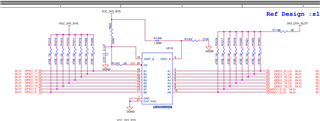
We are using  LSF0108RKSR   for connecting  ARM processor GPIO pins  to other boards to ensure fail safe operation . Both the CPU board and the daughter board runs on the 3.3V logic . So we don't need a voltage level transition , and we are using single supply solution  (image attached).  The issue we are facing is the voltage level at A side pins are clamped by 0.8V . Is there a way to rectify it ? 

in our case only a few pins are Bidirectional rest of the pins are either input or output .

  • Hey Nikhilraj,

    The output waveform seems to suggest the device is functional and output reaching 3.3V. Note that pullups would be required on the output side to see the desired 3.3V since the LSF's outputs are open-drain based and only capable of pulling low. 

    You may also see the TXS0108E supporting VCCA= VCCB =3.3V for simpler implementation without the requirement of the external pullups that the LSF0108 requires. 

    Regards,

    Jack 

  • Hi Jack , 

    Thank you for the response . In the current design we are observing an OFFSET  in the  output  ( when input is 0 , output is 0.8V)   . Output is clamped by 0.8V . This may lead to false trigger the devices connected to the output . Any clue to avoid this offset ? 

  • The LSF creates a direct connection between the A and B pins. When another device drives a line low, it must be able to sink the current through both pull-up resistors (3.3 V / 235 Ω = 14 mA). Apparently, your devices' VOL for such a large current is 0.8 V.

    The LSF is a passive switch and does not provide any isolation (and neither does the TXS). What exactly do you mean with "fail safe operation"? I doubt that the LSF is appropriate in your application.

  • Hi Clemens, 

    "Fail safe operation" is to protect the processor GPIOS . Basically it to ensures no voltage is present in the GPIO lines from the external board when the processor is in booting stage.  A few gpios are bi directional . 

  • So EN1 is pulled low during booting?

    To disconnect the GPIOs, a plain switch like the SN74CBTLV3245A would be cheaper and simpler to use (it does not require pull-ups).

  • Hey Nikhilraj,

    The heightened VOL of 0.8V is determined by the strong pullups and the input VIL at the input of the LSF0108. You may try using weaker pullups to get a reduced VOL. Here is an app note that documents the VIL vs. VOL relationship: Factors Affecting VOL for TXS and LSF Auto-bidirectional Translation Devices

    Devices with tri-state outputs (by driving OE low) or with the IOFF feature (partial-power down mode) will support this "Fail safe operation". 

    Regards,

    Jack