This thread has been locked.

If you have a related question, please click the "Ask a related question" button in the top right corner. The newly created question will be automatically linked to this question.

CD74HC85: Is the reason for the low impedance of RN3 affected by the design parameters of CD74HC85M itself?

Part Number: CD74HC85

Tool/software:


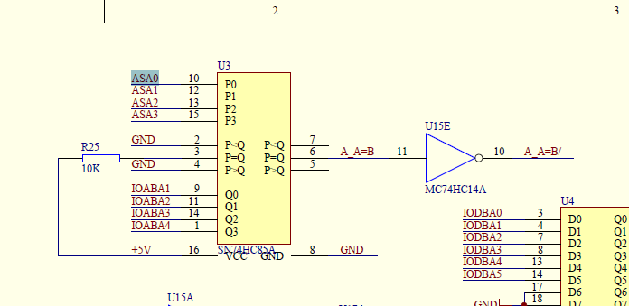
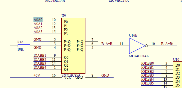
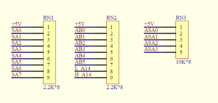
As shown in Figure 3 above, RN3 is connected to the U3 and U9 chips, RN3 is a 10K resistance bar, and U3 and U9 are the chip CD74HC85M. When we measured the electrical rejection impedance at the position of RN3, there were a number of cases where the impedance value was the smallest to 1k, which was directly connected to some pins of materials U3 and U9. We wanted to analyze the reason for the low impedance of RN3, whether it was affected by the design parameters of CD74HC85M?
Some early operations:
1 In batches 1-2, the impedance of the resistance bank was measured directly with a multimeter before the ICT test after the welding was completed, and low impedance was also found.
2 After the normal and abnormal CD74HC85M chips at the RN3 position are removed from the PCB board, the pin impedance connected to the RN3 is measured with a multimeter, which is also different
3. The current treatment method is to directly replace the new materials when there is a deviation in the ICT test, and then test again after the replacement, it can pass the ICT test normally.

  • The four P inputs are high-impedance CMOS inputs, so they should not affect the RN3 measurement in any way as long as U3/U9 are powered and the ASAx voltages do not exceed 5 V. But when U3/U9 are not powered or when the ASAx signals are floating, then the clamping diodes from the inputs to VCC will prevent you from measuring RN3.

  • As described in steps 1-3 above, whether it is the multimeter test before ICT or the ICT test, there was no power on exceeding 5V. Should we understand that when the resistance value of resistor bank RN3 is incorrect, this chip has already malfunctioned or has hidden faults, and needs to be replaced?

    If a functional test is conducted on a chip that is considered faulty or has potential faults when powered on in the system, and only then will the device itself be powered on at 5V, will the functionality of the chip be affected?

    If there is no impact on the functionality of the device, does this chip still need to be replaced?

  • You have not described how exactly your measurements or tests work. The clamping diodes that are in parallel with the pull-up resistors have a much lower impedance.

    As far as I understand, you have two sets of chips that behave differently, and replacing the damaged ones makes the circuit work? There is nothing in a logic input that could damage a resistor. Resistors are much more robust than logic devices, so if the resistors got damaged (probably by overvoltage), then it is very plausible that other devices connected to the resistors also got damaged.

  • We have conducted the following tests:

    After the PCBA board was processed, a multimeter was used to measure the resistance values of 1 (+)~2 (-) and 1 (+)~3 (-) of resistor bank RN3, and it was found that some of the resistance values had deviations. PCBA with large resistance deviation is defined as board 1, and PCBA with normal resistance is defined as board 2

    1) At this point, remove RN3 from board 1 and measure its resistance again with a multimeter. The resistance value is around 10K, and it is preliminarily judged that RN3 is normal. The factor causing the resistance deviation may be CD74HC85.

    2) Remove CD74HC85 from board 1 again, and also remove CD74HC85 from board 2. Comparing the resistance values between the pins of CD74HC85 in board 1 and board 2, there is a difference in their resistance values.

    3) Re solder RN3 and CD74HC85 from board 1 and CD74HC85 from board 2 to the PCBA, and measure the resistance between RN3 pins again, following the same procedure as in step 1). Afterwards, board 1 and board 2 were sequentially placed on the functional testing platform, and both types of boards passed the functional tests.

    4) Place board 1 and board 2 in sequence for ICT testing. Board 1 will report an error of low RN3 resistance, while board 2 can pass normally.

    Question: Is there any impedance difference designed between pins 10, 12, 13, 15, and 16 of this CD74HC85 connected to RN3 at the factory?

  • Pins 10/12/13/15 are high-impedance CMOS inputs. Their resistance relative to VCC and GND should be near infinite. But if you are measuring in the wrong direction, then you measure the clamping diodes with an unspecified resistance (that might differ between chips). In the second case, it would be better to use diode test mode and check whether you get a normal silicon junction voltage drop of about 0.7 V.

    Please specifiy exactly how you are measuring the pins, and what the resulting values are.