This thread has been locked.

If you have a related question, please click the "Ask a related question" button in the top right corner. The newly created question will be automatically linked to this question.

SN74LVC1G04: the input and output signal of converter

Part Number: SN74LVC1G04
Other Parts Discussed in Thread: SN74LVC1GX04

Tool/software:

Hi team:

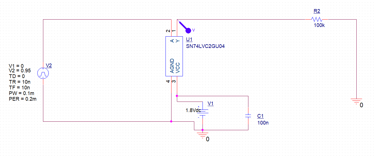
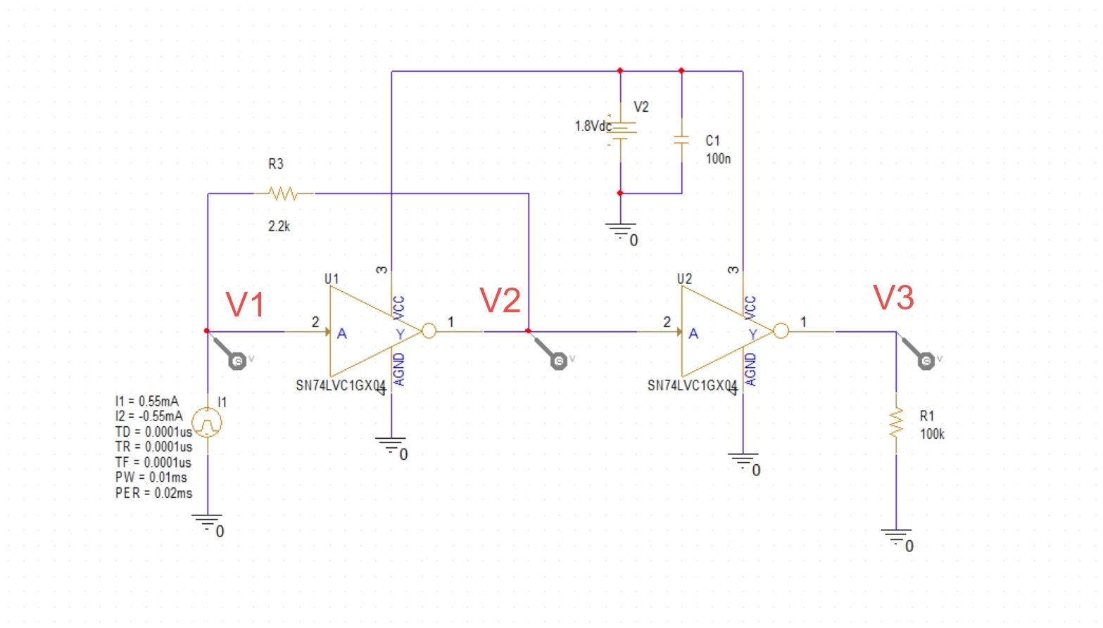
We are currently trying to use two converters to transfer current mode signals (+550uA/-550uA) to voltage mode signals(0V/1.8V), here is the simulation circuit

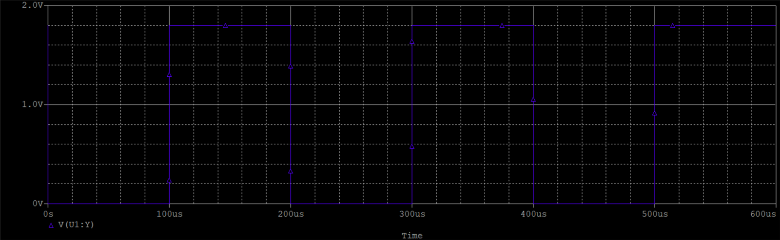
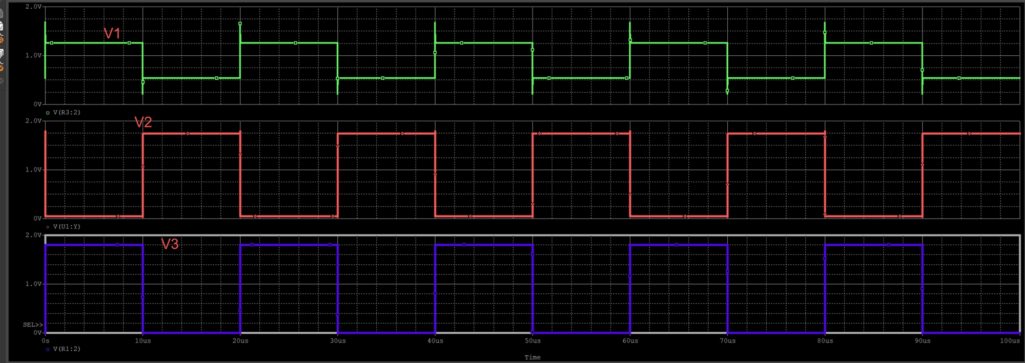
Here is the simulation result, seems the circuit works.

But I have a question about how this inverter works in this circumstance, since CMOS inverter has the topology as following

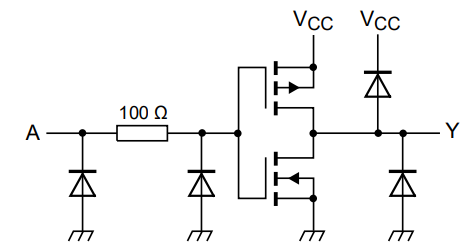
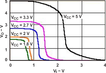
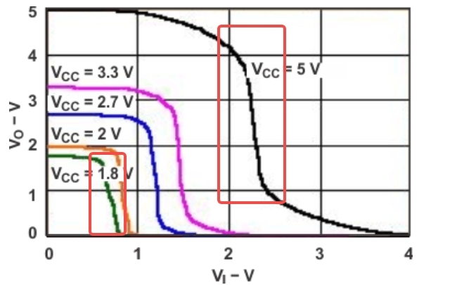
Why there is a bias at the input of inverter, how the resistive feedback causes this bias at gate of two mosfets? this bias is reasonable if it's a OPA, but it's actually a inverter with two mosfets combined. And as illustrated in the simulation result, these bias voltage levels (1.2V and 0.6V) are between VIL and VIH of a inverter, does that mean the first inverter works at transition region?

Could you explain me how this two mosfets combined inverter with a resistive feedback can cause bias at input and eventually resulting the right high and low voltage level at output?

Thanks.

  • An unbuffered CMOS inverter indeed can be used as an analog amplifier in the transition region. Its characteristics are not very good (see figure 7), but it's enough for a crystal oscillator.

    Why are you trying to do this with a logic inverter? A comparator would have much more controlled characteristics.

  • Hi

    This is not for crystal oscillator use, we just use it to transfer current signal (current mode TDM signals) to voltage signal, like TIA amplifier. This solution is suggested by supplier. I am still trying to figure out how this circuit works. My questions are presented above

    What is the open loop gain for this chip specifically? And how to read the curve you posted corresponding to the circuit I posted?

  • The gain is the slope of the curve. It's not linear, and not guaranteed.

    The current generates a voltage drop over R3. This forces U1 to weakly switch either low or high; U2 amplifies this signal.

  • hi 

    Why this resistive feedback forces U1 to have either low or high voltage level output? Could you explain me more in detail regarding the input and output of U1? or does TI has related technical articles?

    And from the simulation result, is not U2 just inverts the output of U1?

  • This depends on how your signal source works (it will certainly not be a theoretical current source like in the simulation). But when a current flows through R3, it will drop ±1.21 V.

    This circuit is suggested by your supplier, so ask them.

    U2 just amplifies the signal, because U1's output might not actually go to the rails. (The SN74LVC1GX04 has a second inverter for that.)

  • hi 

    Thank for your explanation

    I tried to simulate just an inverter to understand VO vs VI characteristics, I found no matter how close to VCC/2 the input is, the output is always either 1.8V or 0V. But from the VCT characteristic of a general inverter, there should be a region close to VCC/2 that both P mos and N mos are in saturation mode, the output is supposed to be divided by P mos and N mos.

    My question is, why I could not get the transition region when output is neither high nor low from simulation, just like the area I marked below

  • It looks as if the simulation model is wrong.

  • So could you send me a link where I can download the right model? I tried both products with one gate and dual gate, it turned out the same result that I could not get the transition region

  • Hi,

    Our team will look into fixing this model