This thread has been locked.

If you have a related question, please click the "Ask a related question" button in the top right corner. The newly created question will be automatically linked to this question.

SN74AVC4T774: What is the maximum SPI frequency it can translate.

Part Number: SN74AVC4T774
Other Parts Discussed in Thread: SN74AXC4T774

Tool/software:

Hi,

I'm trying to run SPI at 50MHz and I need to translate voltages from 1.8V to 1.2V ~ 3.3V.

I'm using the SN74AVC4T774 which works perfectly at up to 30MHz, but when going to 50MHz it seems to fail.

Isn't this IC capable of reaching that speed? I'm a bit confused about propagation delay and transition rise and fall.

The first one should be a problem when translating from 1.8V to 1.8V and the rise and fall time (10 ns/V) should be correct to work up to 50MHz, but under those conditions it's not working.

I tried setting the SPI bus to 3.3V and is also not working.

Any piece of advice?

Regards,

P

  • Hi Pablo,

    Note that the device is specified for up to 380 Mbps (190 MHz) for 3.3 V outputs, 200 Mbps (100 MHz) for 1.8 V outputs and 100 Mbps (50 MHz) for 1.2 V outputs.

    Input transition rise or fall rate spec indicates max of 5 ns / V for all voltage levels. Higher than 5 is not recommended as this will be too slow. Instead of 10 ns / V, use at most 5. 

    Further ensure capacitive load is not excessive. You may confirm by disconnecting all peripherals / components connected to the AVC outputs to verify 50 MHz works.

    For additional support, help clarify what is referred to as failing at 50 MHz with waveforms at the specified output and schematic indicating the test point, thanks.

    Best Regards,

    Michael.

  • Sorry I made a mistake, I'm using SN74AXC4T774. Is this IC capable of handling 50MHz SPI communication? from 1.2V ~ 3.3V input to 1.2V ~ 3.3V output.

    Is SN74AVC4T774 a better IC for this application?

    Regards,

    P

  • Hi Pablo,

    Thanks for clarifying.

    Yes AXC is capable and AVC is a faster device. Would further recommend to verify capacitive loading is not excessive, thanks.

    Best Regards,

    Michael.

  • Hi Michael,

    I only have 1 device connected to the bus, I'm using short wires, I'm using a custom PCB and no protoboard to avoid noises. I am not sure how what else can I do to reduce capacitive load. It should be minimum. 

  • Hi Pablo,

    Could you disconnect the bus and share both the passing and failing waveforms and their respective test points?

    Best Regards,

    Michael.

  • Hi Michael,

    I'm Martin, Pablo's collague.

    First of all, thank you very much for your prompt response.

    After that, I wanted to add some additional comments regarding the issue we are facing. To provide you with a better escenario description, our hardware setup consist of an NXP MCU, the SN74AXC4T774 level shifter and the Mikroe Flash 6 Click board holding an W25Q128JV flash memory. That said, the problem we are facing is that up to 30 MHz/37.5MHz the MCU can read perfectly the data sent by the SPI peripheral (W25Q128JV), but when we increase the frequency to 50 MHz, which is supported by W25Q128JV, the data received by the MCU is 1 bit shifted. Do you have heard about this issue before? Do you have any suggestions?

    Thank you very much in advance.

    Looking forward to hearing form you.

    Best regards,

    Martin

  • Hi Michael,

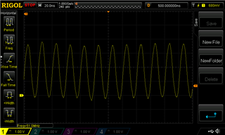
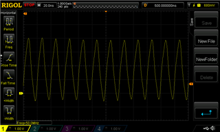
    I'm attaching captures of the input and output signal of the CLK of SPI. Hope they help to sort out the problem together with Martin information50MHz clock input signal50MHz clock output signal

  • I also want to mention that taking the SN74AXC4T774 IC off and shorting An-Bn channels, the communication between the MCU and the SPI peripheral worked correctly as expected at 50 MHz.

  • Hi Martin / Pablo,

    Thanks for clarifying.

    • What is connecting NXP MCU to AXC? Same PCB?
    • What is connecting AXC to Flash? Same PCB? Connectors? Cable?
    • Do you have a block diagram or schematic clarifying? For example, connectors, cables will add additional capacitance.

    A lot of factors may imply what is being referred to as data received by MCU shifting by 1 bit i.e. MCU, pulse width requirement, MCU VOL/VOH requirement, MCU duty cycle requirement, rise/fall time requirement, overshoot/undershoot concerns, etc.

    • Do we know which is impacting the bit shift? 
    • Are the provided waveforms directly from the level-shifter or the MCU as the test point? 
    • Waveforms shown seems to be for input 3.3 V and output 3.3 V? i.e. similar levels (with some overshoot/undershoot). Is this the expected voltage level for the input and output? Please share 30 MHz to clarify impact on voltage levels.
    • Is the waveform shown the passing or failing waveform? Please show both as well i.e. 50 MHz failing when AXC is not removed vs 50 MHz working correctly when AXC is removed. This can help narrow down which factor is most likely the culprit so as to help further narrow down recommendations, thanks.

    Best Regards,

    Michael.

  • Hi Michael,

    I'm attaching pictures of the SPI bus open, sending the 0x9F command (which should answer with the W25Q128JV ID number).

    These captures are with the bus open at 50MHz and at 30MHz.

    SCK and MOSI at 30MHz, after level shifter

    SCK and MOSI at 50MHz, after level shifter

    Regards,

    P

  • Hi Michael,

    Here is the NXP MCU capabilities:

    NXP MCU capabilities

    NXP MCU capabilities 2

    And next is a block diagram of the SPI connection:

    SPI block diagram

    Regards,

    P

  • Hi Michael,

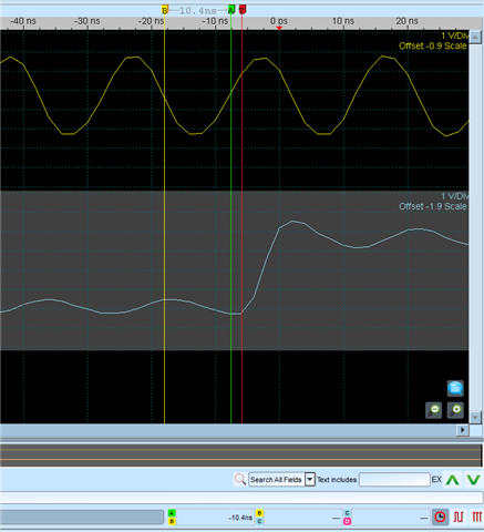
    Here are some captures of the SCK at the input (BLUE) of the level shifter, and the same signal afterwards (SKYBLUE):

    30MHz clock input-output signal

    50MHz clock input-output signal

  • Hi Michael,

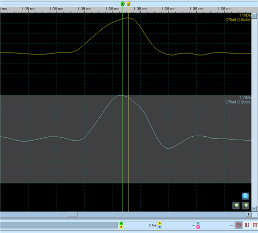
    Here is the last piece of information. I'm attaching a capture of the SPI signals without load and without the level shifter:

    SCK signal no level shifter 30MHz  SCK and MOSI signal no level shifter 30MHz

    SCK signal no level shifter 50MHz  SCK and MOSI signal no level shifter 50MHz

    I hope this can hep to find out why this is not working at 50 MHz

  • The bit shift is probably caused by the propagation delay; when the MISO signal arrives at the master, it is delayed by two times the total transmission delay. The offset relative to the clock signal might have become too large. (In the worst case, 2 × 6 ns = 12 ns corresponds to 83 Mbps = 41 MHz.)

    Your waveforms show slow edges (i.e., the capacitive load is too high) and reflections (i.e., the lines are not properly terminated). Is that block diagram the design of the final product? For high-frequency signals, breadboards or long cables are not suitable.

  • Hi Clemens,

    We connected MOSI and MISO in loopback, so we could measure the propagation delay of the signal at the corresponding pins of the MCU and it seems to be a delay of ~10ns, which is too much for a 50MHz (20ns period) SPI bus.

    When connected the MOSI and MISO signal and measured how long it would take for the signal to come back it was found that it takes too long so when the moment of sampling the bus the lines is still low (for this case) causing this bit-shifting.

    When removed the level shifters there was a delay of ~2ns, and communication worked correctly.

  • Hi Pablo,

    Thanks for clarifying. Could you help confirm the delay from the level shifter output when flat cable | pin board |  Dupont cable | WQ5218JV are disconnected?

    Best Regards,

    Michael. 

  • Hi Michael,

    the pictures from before (the one with the 2ns delay and the one with the 10ns delay were taken with flat cable | pin board |  Dupont cable in loopback connected, the only difference was the level shifter solder (10ns delay) and not soldered (2ns delay)

    that's why I coclude that the level shifte adds too much delay for a 50MHz SPI communication.

    Regards,

    P

  • Hi Pablo,

    Thanks for clarifying.

    Do we know how much delay is observed from the level shifter's output (level shifter soldered) without flat cable | pin board |  Dupont cable | WQ5218JV? 

    You may also disconnect one by one while observing the delay so as to help narrow down the implications of each additional connection.

    I suspect delay will be less. This will indicate flat cable | pin board |  Dupont cable | WQ5218JV adds excessive capacitive loading which will impact delay, thanks.

    Best Regards,

    Michael.

  • Hi Michael,

    MCU -> level shifter -> flat cable -> pin board -> loopback dupont with Level shifter has a delay of ~10ns, without level shifter there is delay of ~2ns. Same configuration, just changes the fact the Level shifter is soldered or not. I think it doesn't matter if I remove, or not, other pieces of the communication path.

    We will proceed by getting the SN74AVC4T774 IC (instead of the AXC version) and try if this new configuration works correctly. This other component its suposed to be faster, correct?

    Regards,

    P

  • Hi Pablo,

    Yes, AVC is faster than AXC.

    Please further note that the other pieces will add to the lumped capacitive loading which will add delay to the communication path, thanks.

    Best Regards,

    Michael.