Part Number: CD4018B
Tool/software:
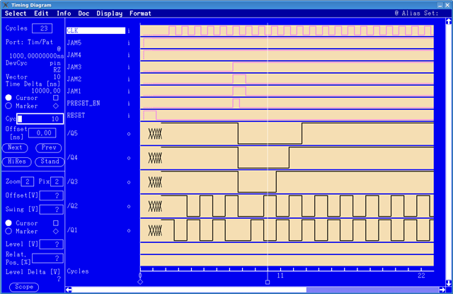
I am currently testing the CD4018BF3A chip and was confused on the functionality of the divide-by-2 configuration. If I'm correct this is simply achieved by connecting the output of /Q1 back to DATA. When I test the chip the outputs I'm getting are:
| CP | /Q1 | /Q2 | /Q3 | /Q4 | /Q5 |
| 0 | 1 | 1 | 1 | 1 | 1 |
| 1 | 0 | 1 | 1 | 1 | 1 |
| 2 | 1 | 0 | 1 | 1 | 1 |
| 3 | 0 | 1 | 1 | 1 | 1 |
| 4 | 1 | 0 | 1 | 1 | 1 |
essentially alternating/toggling between /Q1 and /Q2. Shouldn't the expected outputs be something like:
| CP | /Q1 | /Q2 | /Q3 | /Q4 | /Q5 |
| 0 | 1 | 1 | 1 | 1 | 1 |
| 1 | 0 | 1 | 1 | 1 | 1 |
| 2 | 1 | 0 | 1 | 1 | 1 |
| 3 | 0 | 1 | 0 | 1 | 1 |
| 4 | 1 | 0 | 1 | 0 | 1 |
| 5 | 0 | 1 | 0 | 1 | 0 |
or am I misunderstanding a major concept?
Side note: for a divide-by-4 configuration /Q2 would be fed back to the DATA input and the truth table would look something like:
| CP | /Q1 | /Q2 | /Q3 | /Q4 | /Q5 |
| 0 | 1 | 1 | 1 | 1 | 1 |
| 1 | 0 | 1 | 1 | 1 | 1 |
| 2 | 0 | 0 | 1 | 1 | 1 |
| 3 | 1 | 0 | 0 | 1 | 1 |
| 4 | 1 | 1 | 0 | 0 | 1 |
| 5 | 0 | 1 | 1 | 0 | 0 |
| 6 | 0 | 0 | 1 | 1 | 0 |
| 7 | 1 | 0 | 0 | 1 | 1 |
which is what I would expect but this 'pattern' doesn't reflect for my observed output for a divide-by-2 configuration.