This thread has been locked.

If you have a related question, please click the "Ask a related question" button in the top right corner. The newly created question will be automatically linked to this question.

LSF0108: LSF0108 question

Part Number: LSF0108

Tool/software:

Hello, I'm using LSF0108PWR for level shift. My circuit as below:

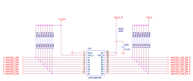
The result I want is:

1,When +V_ADJ = 1.2v, +Vp_A_R=1.8V, +Vp_A = 1.8V, Port A's level 1.2V <------> Port B's level is 1.8V.

2,When +V_ADJ = 1.8v, +Vp_A_R=2.5V, +Vp_A = 1.8V, Port A's level 1.8V <------> Port B's level is 1.8V.

3,  When +V_ADJ = 1.8v, +Vp_A_R=2.5V, +Vp_A = 2.5V, Port A's level 1.8V <------> Port B's level is 2.5V.

4,When +V_ADJ = 1.8v, +Vp_A_R=3.3V, +Vp_A = 1.8V, Port A's level 1.8V <------> Port B's level is 1.8V.

5,  When +V_ADJ = 2.5v, +Vp_A_R=3.3V, +Vp_A = 3.3V, Port A's level 2.5V <------> Port B's level is 3.3V.

6, When +V_ADJ = 2.5v, +Vp_A_R=3.3V, +Vp_A = 2.5V, Port A's level 2.5V <------> Port B's level is 2.5V.

Can the above circuit work for each of the six cases? Thanks!

  • The only LSF requirement is that Vref_A must be the lowest voltage. This is true in all six cases.

  • Thank you, Clemens. The circuit I designed is being made into a PCB board, and I hope it will work well. I try to follow datasheet as much as possible, and it still required Vref_B is 0.8V higher than Vref_A as below. 

  • When the voltage difference between Vref_A and the resistor connected to Vref_B is less than about 0.8 V, then the signal output voltages might not be clamped to Vref_A but to a voltage that is lower. You have pull-up resistors on the A-side outputs, so this does not really matter.

  • Hey Li,

    The above implementations will work, though note that case 1. does not meet the biasing requirement of 0.8V difference between VREFB and VREFA (currently only 0.6V), resulting in the output voltage clamping lower as Clemens suggested. 

    If possible, biasing VREFB to a higher voltage, (i.e 2.5V rail) for case 1. will ensure that the biasing requirement of the LSF is met, and since Vp_A is still biased to 1.8V still, the output signals will be referenced to this voltage as well. 

    Regards,

    Jack 

  • Thank you, Jack. In case 1, we can't change VREFB(+Vp_A_R=1.8V) to a higher voltage. And I have added the pull resistors in Port A and Port B, so it should be able to work without clamping according to the below datasheet. Right?

  • Hey Li,

    Yes still operational, as the external pullups aid the output node up to VREFB voltage.

    Regards,

    Jack