This thread has been locked.

If you have a related question, please click the "Ask a related question" button in the top right corner. The newly created question will be automatically linked to this question.

SN74LV541A: Output Topology

Part Number: SN74LV541A
Other Parts Discussed in Thread: SN74ABT541B

Tool/software:

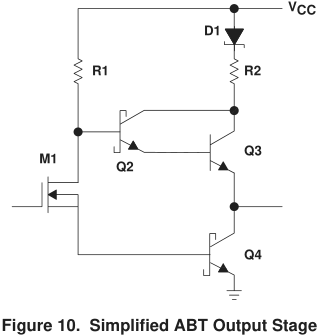
1. What's the topology difference between SN74ABT541 and SN74LV541?

2. Is the output of the SN74LV541AT able to connect to pull-high 5V rail? It looks the abs rating is different for both devices for VO? 

SN74LV541AT => VCC+0.5V; When VCC=0V, the VO derating is only 0.5V~

SN74ABT541B=> 5.5V

Regards

Brian 

  • ABT uses bipolar transistors and allows very high output currents. LV-A is plain CMOS.

    Both devices allow pull-ups when the output is disabled or powered off. (The LV-AT datasheet has a separate limit for that case.)

  • Thanks.

    I'm still confused about the abs max. voltage rating at VO pin. The max voltage rating of the VO pin is addressed as Vcc + 0.5V. When Vcc=0V, is voltage derating is only 0.5V???

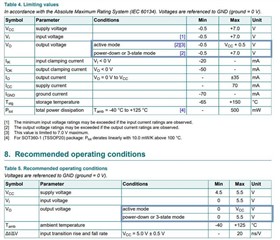
     In the 74LV541AT from Nexperia, customer thinks it is much clear to address the output voltage derating. Please find below with active mode and power-doen mode. When power down mode, max. voltage is up to +7V. It is much easily to understand the voltage stress, isn't? 

  • The ratings of the TI and Nexperia devices are identical.