Part Number: CD4013B
Other Parts Discussed in Thread: CD40106B
Tool/software:
Hello,
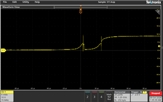
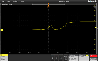
I am prototyping a simple toggle switch utilizing the buffer and D-F-F from the title. They are configured as in Figure 9 from the CD4013B datasheet. The clock signal from the buffer is not as clean as I would expect from a buffered input, and I believe this is why the toggle doesn't work. It has a rise time of about 20us, and gets pulled low as it rises, possibly creating a double clock signal. I have tried placing several different resistors between the buffer output and clock input, as well as RC circuits, but these don't work either and also seem to violate the operating conditions from the datasheet with respect to rise and fall times for the clock input. I should note that this circuit is set up on a breadboard. Any advice is welcome.


