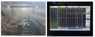
This thread has been locked.

If you have a related question, please click the "Ask a related question" button in the top right corner. The newly created question will be automatically linked to this question.

CD4047B: The CD4047BM96 chip failure issue requires a schematic check

Part Number: CD4047B

Tool/software:

Standard:
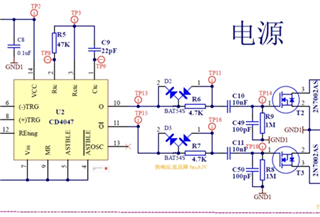
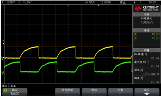
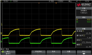
(1) CD4047 requires a power supply voltage range of 3-18V
(2) Power consumption: Power consumption=static power consumption+output current
Static power consumption ≤ 120uA, output control MOS, almost no current on output pins, overall should be far<1mA
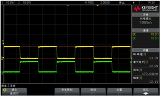
Actual measurement: Approximately 3.3mA, exceeding the specified value at high temperatures

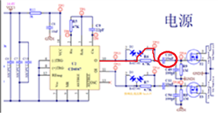
Please help to check the schematic diagram

  • Hi Tony,

    I can't see anything wrong in the schematic diagram. Could you describe more the behavior you are observing resulting in failures? Scope shots of the failing output, and the input driving that would be the best to receive quick help.

    Regards,

    Owen

  • Customer feedback on site: One AM3071EX reported a disconnection fault in the tenth channel of the C-15A chassis during restoration, and the output signal was delayed
    Intermittent continuation; Remove the prototype and retest the AI output and distribution voltage, and the results are OK, as shown in the following figure.


    ① After the defective product is removed from the high-temperature environment, it is immediately powered on and the indicator light goes out for about an hour. CD4047 output is not positive
    Constant: No waveform output, there is a voltage of about 10V on R12;
    ② After the defective product was left in the laboratory environment for a period of time, it was powered on and restored to normal operation using a hot air blower at 150 ℃/wind
    Speed 1: Blow air around the power transformer and the indicator light turns off; (Note: CD4047 is located near the power transformer)
    ③ After leaving the defective product in the laboratory environment for a period of time, turn on the power and the indicator light will turn on [restore normal operation]. Use a hot air blower to clean it
    CD4047 blows air for about 10 seconds, but the output signal is disconnected and the indicator light is off;
    3. Cross validation: Replace the defective product with a new CD4047 and use a hot air blower to blow CD4047. No issues were found after 30 seconds
    Good, replace the normal product with defective CD4047 and use a hot air blower to blow CD4047. After about 10 seconds, the defect appeared,
    4. Cross validation: Replace defective products with new CD4047 and replace normal products with defective CD4047 when placed in a high-temperature environment
    (20 ℃ -60 ℃ -20 ℃ cycle) 4H, continuous monitoring of output signal: replace defective product with new CD4047, normal operation, normal production
    During the process of replacing the product with defective CD4047, there were three instances of wire breakage; As shown in the picture

  • Perhaps this description would be more accurate:

    The customer reported that one AM3071EX unit was experiencing a broken wire fault in Channel 10 of the C-15A chassis, with intermittent output signals. Upon removing the sample for testing, the AI output and power distribution voltage were found to be OK, as shown in the figure below.

    1. High-temperature simulation: The defective unit was placed in a high-temperature environment (20°C-60°C-20°C cycle) for 4 hours, and the output signal was continuously monitored. During the heating process, the output signal was interrupted,

  • Hi Tony,

    After hearing this explanation it sounds like our part was damaged in testing. I brought this to the wider team, and we believe part of the problem is the large capacitor on the output flowing through the diode above the 4.7 K resistor.


    A resistor in series with that diode would prevent a short to ground which is causing the device to draw more power than expected (and potentially damaging it).

    Would it be possible to get some higher quality waveform images? It is pretty hard to discern the behavior from what was previously provided.

    Regards,

    Owen

  • picture 1 (TP13-TP15)

    picture 2 (TP11-TP16)

    picture 3 (TP14-TP18)

    Please help to see if there is any problem. This chip is originally to find the quality for FA analysis, but we need to ask your opinion on the current quality first. Please help to confirm it again, thank you!

  • Thank you. I am looking into this.

  • Hi Tony,

    I don't see any problems in these waveforms.

    A resistor in series with that diode would prevent a short to ground which is causing the device to draw more power than expected (and potentially damaging it)

    This on Port 10 and Port 11 are still my areas of concern for this schematic review.

    I don't see any other obvious reasons for failure here.

    Regards,

    Owen