Other Parts Discussed in Thread: SN65HVD233-EP, , SN74LVC1T45
Tool/software:
Hi,
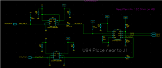
I use Can Bus transceiver PN - SN65HVD233-EP which is connected through a level converter - SN74LVC1T45-EP to FPGA , as shown in the attached drawing .
A level converter side VCCA powered by voltage 2.5V and pin 3 on the device - SN74LVC1T45 connect to FPGA to bank powered from 2.5V , pin 4 of level converter connect to Can Bus transceiver pin 1,
My question is what happens to the output of a level converter pin 4 that connects to the Can Bus pin 1 while the VCCA voltage starts to rise from 0 to 2.5 until the 2.5V voltage stabilizes ?
My suspicion is that until the 2.5V voltage stabilizes, the logic level at the output of the Level Converter component will be in a random state that could disrupt the Can Bus ?
My assumption in this question is that the 3.3V - VCCB of level converter is stable at this time.

Thanks,
Evgeny


