This thread has been locked.

If you have a related question, please click the "Ask a related question" button in the top right corner. The newly created question will be automatically linked to this question.

UCC14140-Q1:

Part Number: UCC14140-Q1

Tool/software:

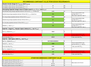
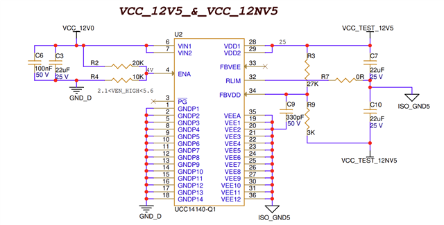
Hi, I am using UCC14140-Q1 to generate both +12.5 and -12.5  and i want same current in both voltage rails

  1. Will the below circuit work perfectly?
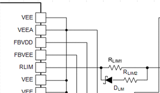
  2. Did I need to add RLIM and DLIM? if yes can you please suggest me part numbers.
  3. Should I need to add more capacitor between VCC_TEST_12V5 and ISO_GND5 /ISO_GND5 and VCC_TEST_12NV5

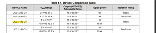
  • In the datasheet, it showed that its output will be either 1W or 1.5W. I want to know exactly how much power and current I can expect.

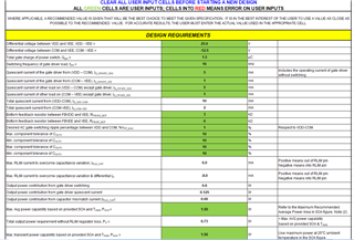
  • I have used the UCC14140-Q1 calculator and filled in all the details. Can you tell me if these are correct? If I do not add any Rlim resistor, will it work or not? The calculator shows a warning in red.

  • Hi Rakesh, please see my feedback below:

    -Design Calculator:

    a. (COM-VEE) voltage should be positive +12.5V, not negative value.

    b. The top feedback resistor of FBVEE can not be 0kohm. You need to use FBVEE pin to regulate (COM-VEE) voltage. Use a 10kohm connected between (FBVEE-VEE). The calculator will tell you the value of the top resistor.

    c. Your output power requirement is ~0.7W. The recommended average power of UCC141410-Q1 is 1.5W, so you are in good shape regarding power capabilities.

    d. RDR configuration is recommended. That helps to reduce the losses through Rlim resistor when using just Rlim. Please, follow recommended values from Calculator after correcting a) and b).

    e. Gate driver caps: Cout1b is recommended to decrease gate driver caps values (VDD-COM) and (COM-VEE) and improve the balance at COM net. Select Cout1b value in Calculator and then follow recommendations for gate driver caps after correcting a) and b)

    f. Finally, you can send your updated Design Calculator and Schematic to be reviewed.

    Thank you

  • Hi Manuel Alva Hernandez,  
    Thank you for your response. I have attached the updated schematics. Can you please review them and provide feedback on whether any modifications are required?

  • I have changed the 0 KOhm resistor connected between RLIM and ISO_GND5 to 1 KOhm resistor is it ok

  • Rakesh. Please, see my feedback below:

    -RLIM cannot be zero, especially if you have quiescent current coming from other loads different than the gate driver. I recommend using RDR configuration as it helps to decrease conduction losses compared to a single RLIM configuration. Please, follow RDR recommendation values from Calculator Design.

    -I recommend increasing the voltage rate of your gate driver caps C7 and C10 to ~35V to prevent DC bias rate.

    -Add a 100nF, X7R, 50V HF decoupling cap next to (VDD-VEE) pins. I recommend placing it next to the output pins as a good practice so that it reflects the position of the cap in the layout. You can place the 2x22uF next to the 100nF cap. See example below from EVM.

    -Swap positions of C3 and C6 so that 100nF cap is placed next to input pins (VINP-GNDP). Similar than above, this is a good practice to reflect the position of the caps in the layout. See example below from EVM.

    -330pF feedback caps are recommended to be placed next to the IC. You can also place them in parallel and at the left side of bottom feedback resistors. See example below from EVM.

    Thank you