


Part Number: TXV0106
Tool/software:
Hi,
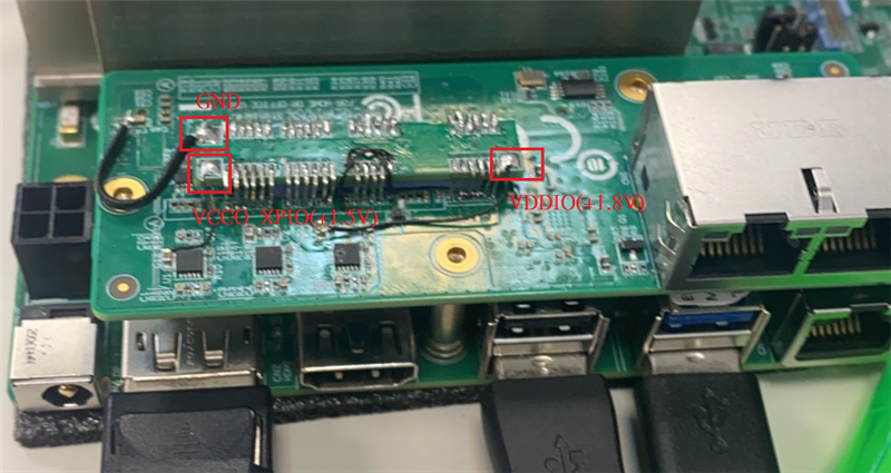
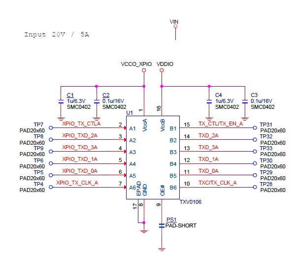
We created a small board to stack on top of the original daughter card to validate the TXV0106 (as shown in the image below). The circuit is straightforward, as below figure, we have use 4 TXV0106, I will pass full schematic via privacy message.
We are currently facing an issue:
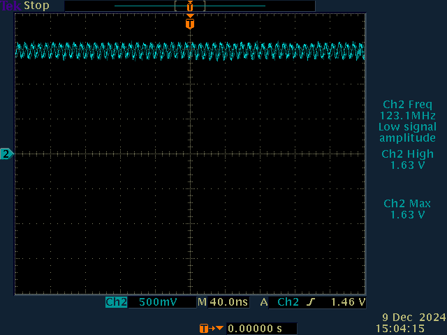
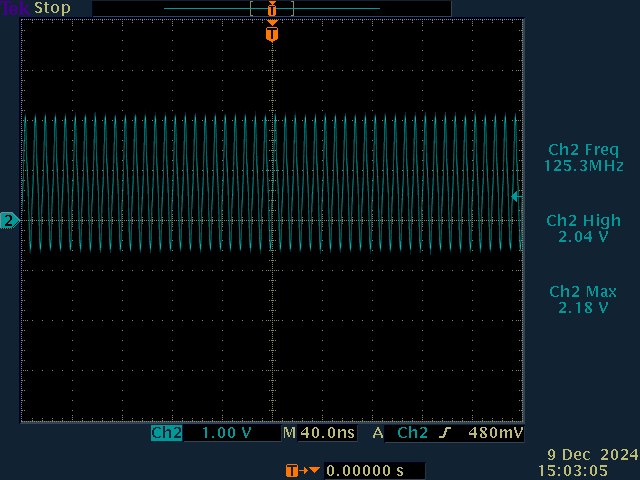
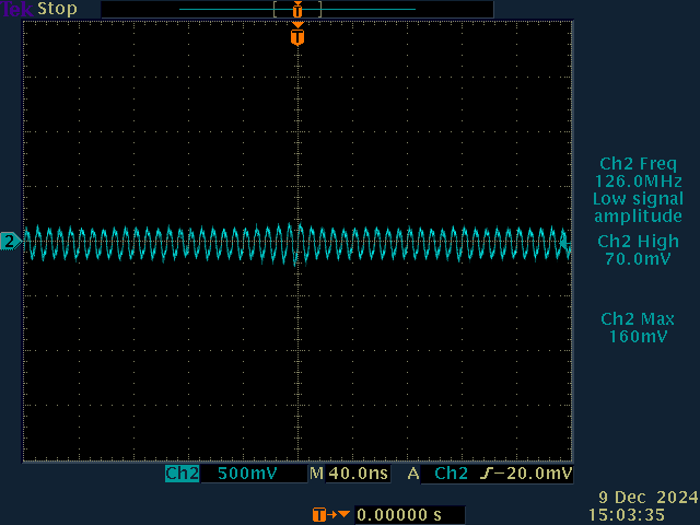
When the TXCLK on side A (input) of the TXV0106 is 125MHz, the TXCLK on side B (output) (refer to the attached TXCLK.BMP) is also 125MHz. However, the small board's GND (GND.BMP) and POWER ( VCCO_XPI.BMP) become abnormal, as shown in the attached files (VCC_XPIO.bmp and GND.bmp), which in turn affects all other signals (e.g., RXCLK_OUTPUT.BMP).
When the TXCLK is reduced to 2.5MHz, all signals return to normal (refer to RXCLK_Nor.BMP).
Or, if I disconnect the TXCLK output on side B of the small board (i.e., not connected to the PHY on the daughter card, but TXCLK still outputs), the issue does not occur.
1.VCC_XPIO
2. TXCLK
3. RXCLK_OUTPUT
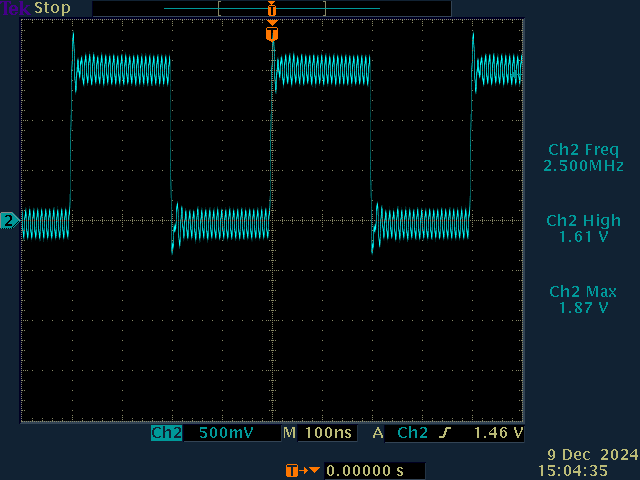
4. RXCLK_Nor

5.GND
Do you have any suggestions on how to resolve this problem?
Thanks!
Jeff

