This thread has been locked.

If you have a related question, please click the "Ask a related question" button in the top right corner. The newly created question will be automatically linked to this question.

SIMPLESWITCHER-COMPONENT-CALC: DRV5055A3QDBZR

Part Number: SIMPLESWITCHER-COMPONENT-CALC

Tool/software:

To dear sir who concerned,

I have a question about the components DRV5055A3QDBZR, please see my attached datasheet for this components.
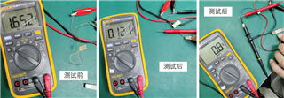
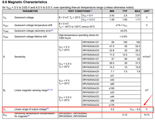
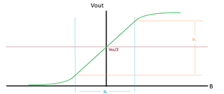
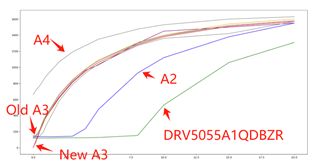
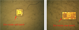
You can see that the linear range of output voltage is between 0.2 to Vcc-0.2V, however In fact, the result of our test is about 0.121V, and some will even reach to 0.008V, please see picture a below, The first picture is the data before testing, the second and third picture is the data after testing. Our customer is now complaining why the test data is so mucu lower and will lead to the product function NG, can you pelase help to check and advise?

I am looking forward to receiving reply very soon, thanks.

 drv5055 (EN).pdf

  • Hello Becky

    Thanks for writing to us.

    I will forward this to our sensing team. Responsible application expert will reply to you soon.

    Thank you

    Regards

    Onkar Bhakare

  • Becky,

    Thank you for reaching out on E2E.  I see there may be some misunderstanding what is meant by this specification.

    The linear output range refers to where all devices can be reliably expected to drive the output before entering saturation.  While it may be possible that each individual device may drive the output to a value beyond this point, you will find that the device does not do so linearly.  The slope of the output curve will begin to taper towards this maximum level.

    BL and VL are related to one another through the sensitivity of the selected sensor.  

    Thanks,

    Scott

  • Hi Scott,

    We've been using  the DRV5055A3QDBZR in our product for years, sourcing it from various distributors.  Recently we have encountered a critical issue with the newer batches, as they exhibit different performance charateristics compared to the older ones. Specifically:

    1. The lowest output of the older ones is approximately 110mV which aligns with your spec. But for the newer batch, the lowest output can drop to as low as 10mV. Please refer to the following measured output diagram to see the difference:

    2. We decap the old and new batch IC, found the die looks quite different. Please see the following picture:

    So my question is: is this newer IC your new design or is it just fake?

  • Becky,

    I would like to discuss this with you further through email to verify you do have the correct material.  I will send a response to the email account associated with your myTI account.

    Thank you,

    Scott