Tool/software:
Hi Team,
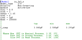
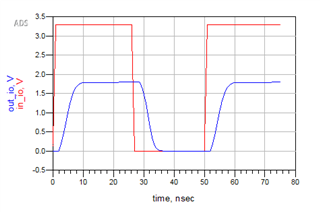
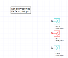
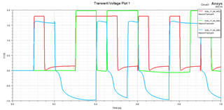
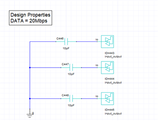
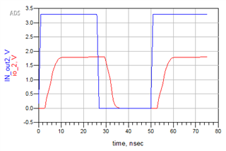
Using the level shifter, we are simulating an SPI interface which translates from 3.3V to 1.8V. @20Mhz
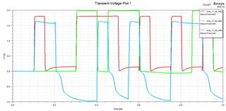
The waveforms at the output of Level shifter seems to be improper.
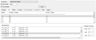
The signal low seems to be dipping to -0.5V using the IBIS model from the TI website.
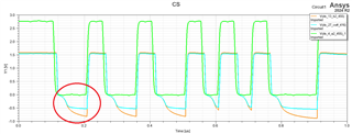
And also, this occurs only at Slow corner of the simulation alone.
Please do provide your comments on this.
Thanks and regards,
Sathish Raja C
Hello Sathish,
Is it possible to share your schematic with us? Another recommendation we usually give is using the AXC4T774 EVM for additional testing.
I've ran the AXC4T774 may times from 3.3V to 1.8V and never seen an undershoot like the one you are showing.
Regards,
Josh
Which pin model did you use? I did not see anything unusual in the 1.8 V model (io_1p8_y).
I am using the below models for my simulation:
io_1p8_x for 3.3V to 1.8V
io_3p3_y 1.8V to 3.3V.
Hello Sathish,
Please allow us some time to look into this. Thanks!
Regards,
Josh
Sure..But please do reply us within this week as we there are some deliverables ON-HOLD due to this.
Thanks,
Sathish Raja C
Hi Joshua,
Any update on the above issue faced.
Currently the model is rated for 130C @slow corner can we get the model for 100C.??
...
Do provide your response ASAP.
Thanks and regards,
Sathish Raja C
Hello Sathish,
Apologies again for the delay. After trying different IO models, I am not able to replicate the waveforms your shared. Below is the waveform for the io_1p8x model. Can you share the components connected to the output?
As for 100C for Slow PVT, unfortunately we won't be able to provide this at this time.
Regards,
Josh
Hi Joshua,
Attached are the IBIS model of TX (saa-tc4d9xe-20mf500.ibs) and RX (m70a_spi_aat.ibs)
m70a_spi_aat.ibssaa-tc4d9xe-20mf500.ibs
Below is the topology of SPI for ref
Thanks and regards,
Sathish Raja C
Hello Sathish,
We are taking a look at this and will provide an update by EOD Friday. Thanks!
Regards,
Josh
Hello Sathish,
Similar as before, I have not been able to replicate the issue. Waveform captures when AXC output is connected to the NAND Flash input (CS) is normal. Additionally, I have not seen this issue (heavy undershooting) on actual silicon before.
Regards,
Josh
Hi Joshua,
Can we have a call to discuss on the issue faced by us.
Do setup a teams call considering IST zone.
Or do provide a convenient time will setup a call.
Thanks and regards,
Sathish Raja C
While ringing is possible, it is not possible for this device to generate a DC voltage below GND. So this must be a problem with the simulation, not with the real device.
Please specify which IBIS simulation software you're using, and how exactly you have configured the load at the output pin.
Hello Sathish,
I agree with Clemens here, please provide a visual on how the output pins are configured. Load capacitance, transmission line impedance, transmission line delay and so on can impact the output signal and cause ringing.
Regards,
Josh
hello
please to find my configuration under ansys Desktop version2022R2
the simualtion is done without load with the gate but in the three modes Typical / Slow / Fast
ID 443 in typical; ID 444 in Fast ; ID 445 in slow
Without load :
the results get are the following
With load of 10pF:
regards
Yannick
Hello Yannick,
A 10pF load capacitance is very common and shouldn't be causing heavy undershoot. You have "io_1p8_x" model but what pin are you using?
ADS is the software program we use and I'm able to select pins and models.
Regards,
Josh
Hello Joshua
i am sorry. With Ansys' desktop we can also select the model in these simulations. We used this confg ip8_x in the three modes :
IO_
Regrads
Yannick
Hello Yannick,
I went ahead and changed the component and pins to match your settings. However, I still was not able to replicate the waveforms you showed us.
Is there more to the IBIS model (ID=443) you shared? The IBIS model I get when using ADS looks something like this:
Can you share how you are referencing this IBIS model?
Regards,
Josh
Hello Joshua,
I don't have other element I can share because there isn't other elements like ADS.
For the reference, i can't change it, So i assume it is GND.
I made the same test on Hyperlynx and I got the same results that you. so it is probable that the error from ansys.
regards
Yannick
Hello Yannick,
Yes, I agree the error may be coming from ansys but I would still recommend sampling the device in a prototype board to eliminate any concerns.
If there are any questions in the future, please feel free to reach out. Thanks!
Regards,
Josh