Other Parts Discussed in Thread: SN74AHC541, SN74LV541A
Tool/software:
Hello. I have a question regarding the SN74LV8T245 octal bus transceiver. We are using this device to translate from +5V (B-side) to +3.3V (A-side) I/O. The circuit diagram is below:
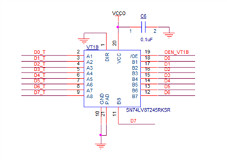
This device is actually on an adaptor that sits on a host board. On the host board the D0~D7 lines are pulled up to +5V with 10K pull-up resistors. The setup is shown below (one channel):
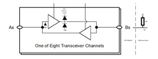
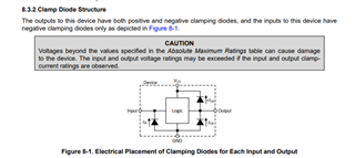
The problem we are finding with this setup is that the VCCO (+3.3V) voltage rail is being pulled up to +4.2V. It appears that the combination of the pull-up resistor and the upper clamp diode of the A-side output buffer provide a path from the +5V rail to the +3.3V (VCCO) rail.
Please could you comment on this.
The SN74LV8T245 voltage translator VT1B is correctly configured for translation from +5V to +3.3V. Pulling up a databus line to +5V with a 10Kohm resistor is typical practice.
I notice that TI have other voltage transceivers. If I selected one without clamp diodes i.e. the SN74AHC245RKSR or the SN74LV245ARKSR, would this solve the problem?
Thanks.