This thread has been locked.

If you have a related question, please click the "Ask a related question" button in the top right corner. The newly created question will be automatically linked to this question.

LM5116: LM5116 as current limiting IC, working and logic as how it limits the current.

Part Number: LM5116

Tool/software:

Hi Everyone,

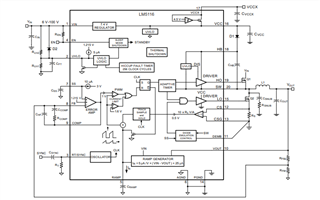
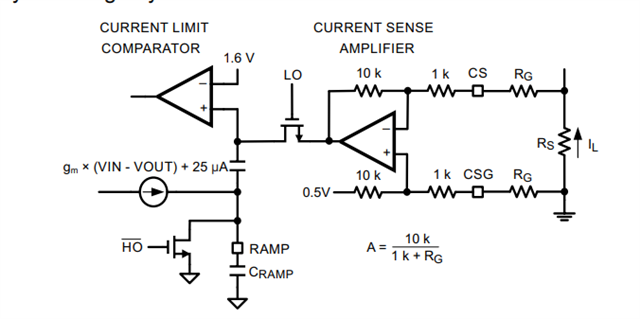
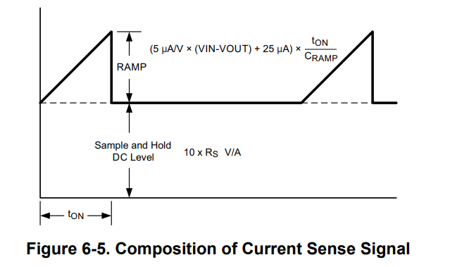
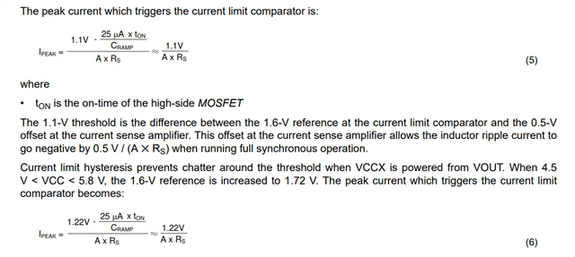
We need to know how this LM5116 is limiting the current? 

How does this IC triggers and protect the circuit when the current between Vin and Vout is reached to its specific current limit? It should limit the current when the HO is turned On & when the LO is turned On after HO is turned off i.e. during both cycles of the Inductor.

Please explain and lets us know the logic and calculation as how this is limiting the current between Vout & Vin during different conditions.

  • Hello Chahak

    The device implements cycle by cycle current limiting. Emulated ramp signal being the representation of the actual peak inductor, it is compared with current limit comparator. If emulated peak cross 1.6 V current limit comparator triggers and device turns off top switch. Device also has hiccup mode to protect it further, it is initiated if current comparator triggers for 256 consecutive cycles.

    I would recommend referring 6.3.7 Current Limit for more details and calculation procedure.

    You can also check QuickStart for the device to ease design process LM5116-5116WG-25116DESIGN-CALC Calculation tool | TI.com

    Thank you

    Regards

    Onkar Bhakare

  • Hi Mr Onkar,

    Thanks for your reply.

    Emulated ramp signal is to control the PWM accordingly and the amplified differential signal between CS & CSG pins will be fed to the current limit comparator which will trigger the comparator if the peak of this amplified differential signal crosses 1.6V.

    Ramp signal is to ensure that the duty cycle (D) of PWM is in proportional to the Vin-Vout and when the Vout-Vin, the duty cycle is reduced to zero.

    Is this the right approach?

  • Yes Chahak 

    You are right!

    Emulated ramp is representation of inductor peak current. Instead of sensing peak current directly IC is emulating it by generating ramp signal and the signal will be compared to get the duty cycle.

    Working principle is similar to peak current mode control except peak is emulated by using Vin, Vout and L information.

    Thank you

  • Hello Chahak

    Let me know if you have any further questions. Kindly close the thread you feel your query has been answered.

    Thank you

    Regards

    Onkar Bhakare

  • Hello Mr Onkar,

    Thanks for your replies.

    I already know the theory that we are discussing here, I want to know the mathematical equation which is being compared to the 1.6V.

    Ramp signal is proportional to Vin-Vout along with a offset of 25uA. 

    But I want to know the maths of the same. As how this ramp signal is being converted into voltage and are there any other signals affecting the same. 

    And most importantly the final equation which is being compared to 1.6V. 

    Please share us a little more than that is already being present in the IC datasheet.

    Thanks & Regards,

    Chahak Godara

  • Hello Chahak

    Thanks for following up!

    But I want to know the maths of the same. As how this ramp signal is being converted into voltage and are there any other signals affecting the same. 

    Current proportional to (Vin - Vout) and slope current (25uA) is forced into Cramp capacitor to converter it into voltage. This voltage signal is equivalent to ΔIL. This signal will get DC shift when it is added with current sense amplifier through bypass capacitor 

    Equivalent signal will be as shown in the figure

    And most importantly the final equation which is being compared to 1.6V. 

    Following equations has been derived from the same principle and it should be used to calculate the trigger point for entering in current limit.

    I hope this answers you questions

    Thank you

    Regards

    Onkar Bhakare

  • Hello Chahak

    I would recommend you using quickstart for the device to ease the design process. You can find it here -  LM5116-5116WG-25116DESIGN-CALC Calculation tool | TI.com

    L
    et me know if you have any further questions or need clarification

    Thank you

    Regards

    Onkar Bhakare