Other Parts Discussed in Thread: TXU0104
Tool/software:
I am using the TXS0108E and have observed some expected behaviour:
1. I have sett VCCA = 1.8V and VCCB = 3.3V, but the B-side outputs have a magnitude of 2.5V - I was expecting 3.3V.
2. I have connected the A side of the TXS0108E to an FPGA 1V8 bank and have confirmed the correct logic values on the A side of the device, however, some of the equivalent B-side outputs have the opposite logic state - this is not what i was expecting.
In all cases, OE has been pulled-up to VCCA to enable all the I/O
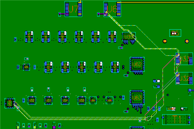
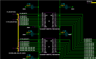
my schematic is as follows:
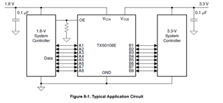
I believe my schematic is identical to the diagram below from the datasheet
please advise ...
thank you