Part Number: CD40109B
Tool/software:
Hi
When operated in the mode VCC > VDD, the CD40109 will operate as a high-to-low level-shifter. In this situation, what are the logic levels for the "Enable" pin?
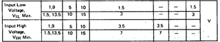
In fact I am not 100% sure what this logic level level is generally - is it (0.7* / 0.3*) Vdd for instance? I do not understand the lower part of the table "STATIC ELECTRICAL CHARACTERISTICS".
For example, the column "Vo" and the entry "1,9": What does this "1,9" signify? - I assume Vo must be short for Voltage Out.
In my case, I have 2 chips:
- One is acting as 5v (in) --> 9v (out).
- One is acting as 9v (in) --> 5v (out).
What are the ENABLE logic levels here. Is 5V fine in both cases, or does case (2) need 9V?
Regards
Stephen