


Tool/software:
Hello,
We are currently using the SN74LVT162245ADL in our design to send data signals between the FPGA and a Flash device.
It seems like we are having issues reading from the flash.
So the FPGA signals are connected on the "A" Side and the Flash device is connected to the "B" Side.
VCCA is 2V5 and VCCB is 3V3. The DIR and OE signals are controlled by the FPGA. Both DIR 1 and 2 share the same signal. The same with OE.
So when we send the write signal (A => B), the FPGA signal looks correct, and the output to the Flash looks correct as well. It is properly translated. However, only on some pins, we noticed incorrect behavior of the data being outputted towards the FPGA (B => A).
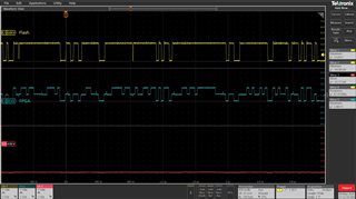
You can see below, that CH1 at the pin of the B side. CH2 is the corresponding pin on the A side. CH3 is the DIR signal.
Here are things that we have already done:
1. We replaced the device, but the same pins still have the same issuse
2. We noticed during active operation there is a impedance difference from a working pin and a non working pin. A working pin would have around 0.92MOhm but a non working on is around 0.89MOhm. But we only see this difference when we have the board powered on. When its off the resistance measures the same between working and non working pins
3. We have tried a different board, and it is interfacing correctly and when we measure the impedance we get 0.92MOhm on the same pins that are not working on the suspect board.
Thanks
Albert

