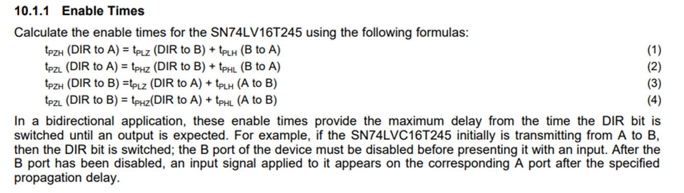
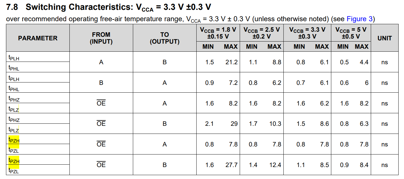
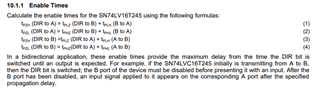
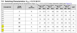
This thread has been locked.

If you have a related question, please click the "Ask a related question" button in the top right corner. The newly created question will be automatically linked to this question.

SN74LVC16T245: 10.1.1 Enable Times

Part Number: SN74LVC16T245

Tool/software:

Hi all,

I would like to confirm about ''10.1.1'' .The usage conditions are Vcca=3.3 V, Vccb=5 V.

It is defined as below, but where are the propagation delays (DIR to A) and (DIR to B) defined?

I saw the answer in the related E2E, but I could not understand it well.

(+) SN74LVC16T245: questions about datasheet section 10.1.1 - Logic forum - Logic - TI E2E support forums

For example, if I want to know tPZH (DIR to A), can I refer to the time below?

Best Regards,

Ryusuke

  • Yes; the DIR and /OE control inputs behave in the same way.

  • Hello Ryusuke,

    I agree with the response from Clemens.

    Let us know if you have further questions.

    Regards,

    Josh

  • Hi Joshua and Clemens,

    Thank you for your reply.

    I understand that (DIR to *) should refer to nOE of FROM INPUT.

    If the above is correct, Should I refer to the left side or the right side of the equation below?

    I think the contents of the equation do not match the parameter of 7.8 Switching Characteristics: VCCA = 3.3 V ±0.3 V.

    Best Regards,

    Ryusuke

  • The test conditions are different. For section 7.8, see figure 3. The equations in section 10.1.1 are for a different case, when the signal that goes in the other direction also has a different value. For example, if the direction originally is A to B, and the input and output pins are both low, and the direction is switched, then you first have to wait for pin B to be deactivated, and then for the low B signal to be propagated to A. This case does not actually happen in practice because you would not want to have two devices driving the line at the same time.