This thread has been locked.

If you have a related question, please click the "Ask a related question" button in the top right corner. The newly created question will be automatically linked to this question.

SN74LVC8T245: Power Sequence Requirement

Part Number: SN74LVC8T245

Tool/software:

Hi team,

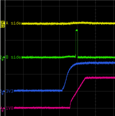
SN74LVC8T245 datasheet has power-up sequence requirement below.

> ”The recommendation is to first power-up the input supply rail to help avoid internal floating while the output supply rail ramps up. However, both power-supply rails can be ramped up simultaneously.”

Is there any specific timing recommendation or acceptable timing range to power up output supply rail on this?
The potential risk of violating the power-up sequence is just undefined output, correct?
I'd like to make sure it won't damage the device.
I found many thread related to this, but it's difficult to find all information my customer is asking for.

Best regards,
Kazuki Itoh

  • Hello Kazuki,

    It's always recommended to force I/Os into a Hi-Z state during power up/down to prevent unwanted glitches from occurring. This can be done by tying /OE pin to VCCA.

    If your data flows from A to B, then it's recommend to power VCCA first or both VCCA and VCCB at the same time.

    Similarly, if data flows from B to A, then it's recommend to power VCCB first or both VCCA and VCCB at the same time.

    Regards,

    Josh

  • Hi Joshua,

    Thank you for providing the information. But could you answer my customer's questions one-by-one?

    1. Is there any specific timing recommendation or acceptable timing range to power up output supply rail on this?
    2. The potential risk of violating the power-up sequence is just undefined output, correct?
    3. Does the violation of the power-up sequence potentially damage the device?

    Best regards,

    Kazuki Itoh

  • Hello Kazuki,

    1. No specific timing recommendation.

    2. That's correct. When I said unwanted glitches, this is what I mean:

    This was taken from another E2E thread but the topic is similar. 3.3V supply (output buffer) is powered up first which creates an unwanted glitch to appear on the output side.

    3. No potential risk for damaging the part.

    Regards,

    Josh