This thread has been locked.

If you have a related question, please click the "Ask a related question" button in the top right corner. The newly created question will be automatically linked to this question.

SN74LVC1G07: Output configuration

Part Number: SN74LVC1G07
Other Parts Discussed in Thread: SN74LVC1G04, CSD15380F3

Tool/software:

Hi Team,

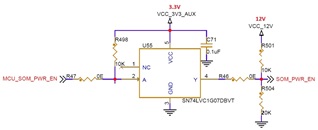
 I'm using SN74LVC1G07DBVT for a reset signal in a development board. Since SN74LVC1G07DBVT is a open-drain non-inverting buffer, can i have the pin 4 (Y) output pin connected to the destination without a pullup , to get a Hi-impedance state or low corresponding to input as high or low respectively. Is this a right approach, does this will affect the device functionallity bt any chance ? Pullup in output side is must?

Regards,
Anoop

  • Without a pull-up, you will never get a high voltage on the reset line. You need only one pull-up on the entire line.

  • Hi Clemens,

    Thank you for your reply. Please find the attached image for your reference. Is it okay to have a voltage divider at the output?

    Regards,
    Anoop

  • A voltage of 8 V at the output exceeds the absolute maximum ratings and is likely to damage the device.

  • Hi Clemens,

    Would changing the resistor from 20K to 10K bring the voltage down to 6V, which is within the absolute maximum rating? Also, would operating the device under this condition for an extended period be considered reliable?

    Regards,
    Anoop

  • What is the actual problem you're trying to solve? What are the requirements for the SOM_PWR_EN signal?

  • Hi Clemens,

    The requirement for SOM_PWR_EN is that it should be an open-drain output from the development board, as I mentioned earlier. A pull-up is present on the module, which is inserted into the development board. This signal is used to power down the module when the line is pulled low by the carrier board.

    As referenced in the schematic, a 10kΩ and 20kΩ voltage divider is present on the module side, with 12V as the source. If I connect the output pin of the SN74LVC1G07DBVT directly to the module’s SOM_PWR_EN, it may damage the SN74LVC1G07DBVT due to the elevated voltage level.

    To address this, I am planning either to add a 10kΩ pulldown resistor on the development board, which would form a new voltage divider resulting in approximately 6V — within the absolute maximum rating of the SN74LVC1G07DBVT — or to use a Schottky diode on the output pin instead of resistor R46. Please provide your feedback on this approach and let me know if there is anything else I should consider.

    Regards,
    Anoop

  • With a pull-down resistor, the signal would no longer be open-drain. A diode would not protect the output against high voltages.

    Just use a discrete transistor (e.g., CSD15380F3) driven from an inverter (e.g., SN74LVC1G04).