Tool/software:
Might it be possible to help us with this rather urgent question. We have a design review Thu 7/3 and this question came up.
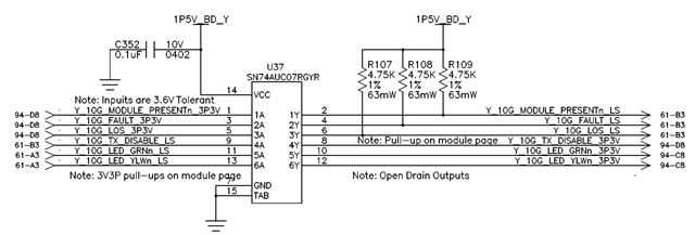
The SN74AUC07 is 3.3V IO tolerant as per its datasheet. We are inputting several 3.3V logic signals as well as several 1.5V logic signals applied to the inputs, thinking it’s 3.3V tolerant for IO. Is this correct even if the part is powered from 1.5V? Also, the 3.3V (logic source supply) and 1.5V supplies are sequenced together, but there is no guarantee that there is not some delay between them, perhaps 10s of uS since they both ramp up from different supplies.
Did we do something wrong in this implementation? Is it risky? A change at this point would be rather painful since we have a number of them formulated similarly. Still, we need to do what is workable.
Can you possibly get us an answer Thu am for this one. We would be very grateful.