This thread has been locked.

If you have a related question, please click the "Ask a related question" button in the top right corner. The newly created question will be automatically linked to this question.

SN74AUC1G14: SN74AUC1G14

Part Number: SN74AUC1G14
Other Parts Discussed in Thread: SN74AUP1G14, TLV809E

Tool/software:

Hello,

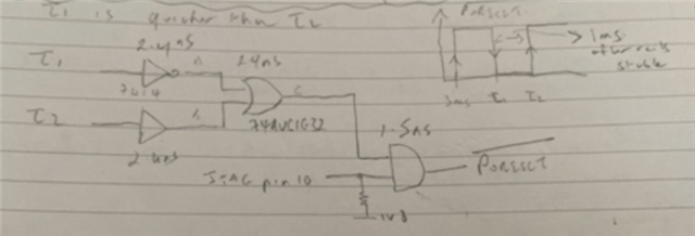
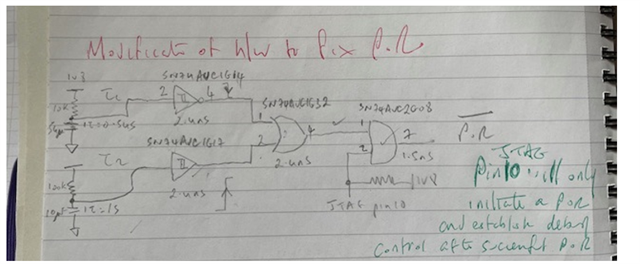
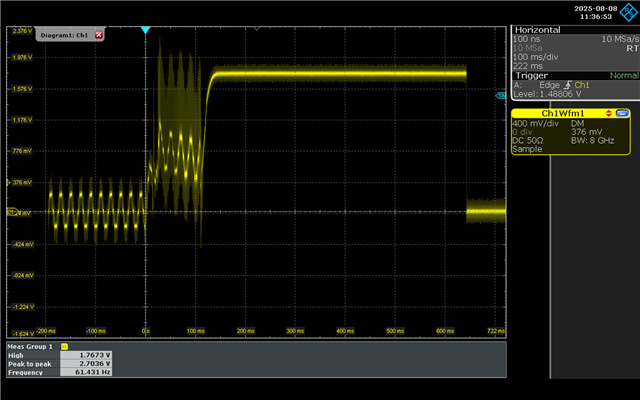
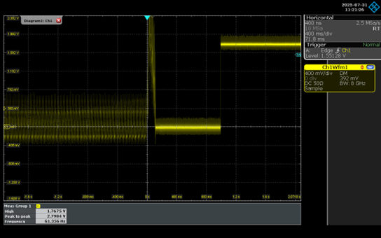
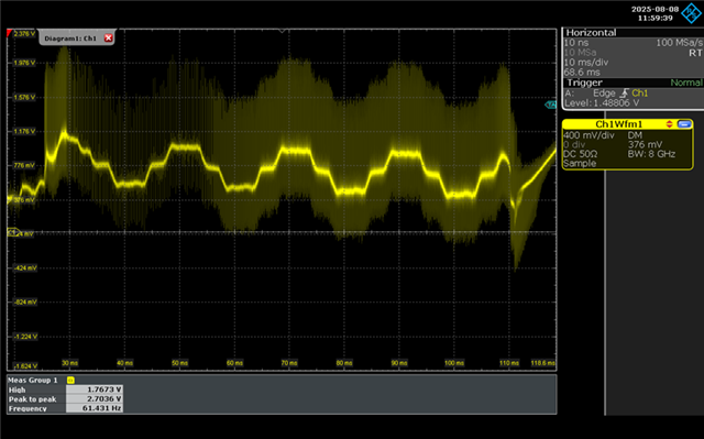
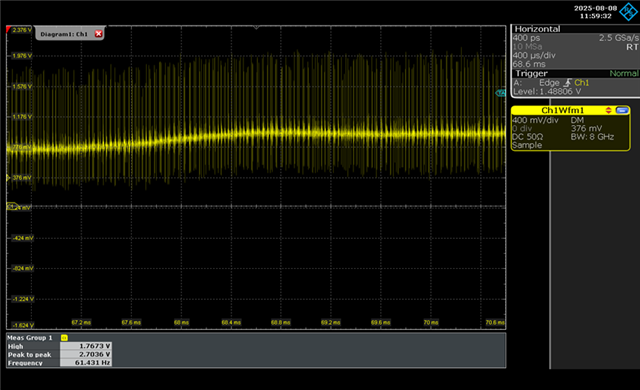
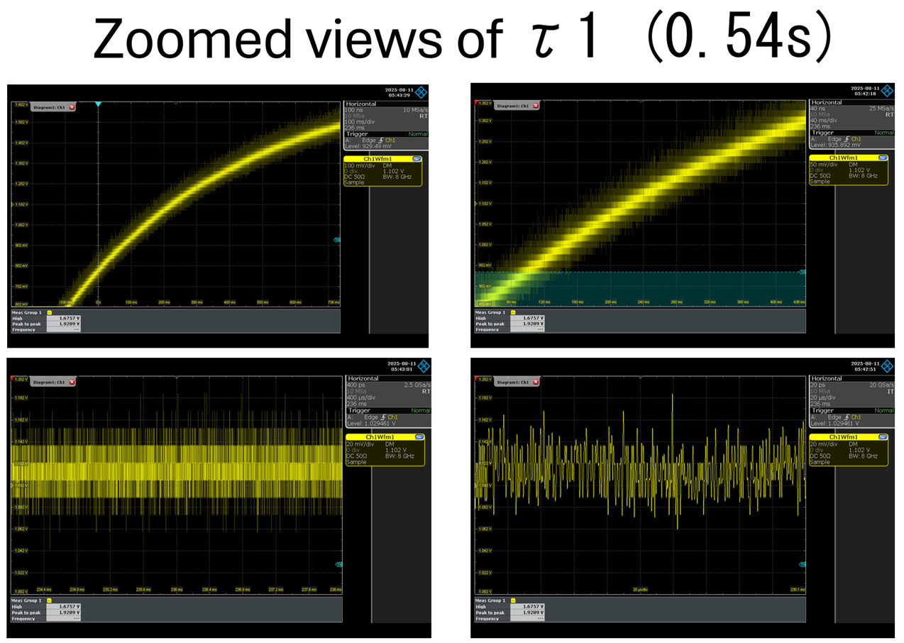
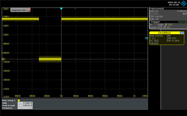
I wish to use a SN74AUC1G14 inverting buffer powered using 1V8: from the datasheet, VT+ is approx. 0.9V and VT- is approx. 0.5V respectively.

If I input a slow rising power-on-reset signal to SN74AUC1G14's input, can you confirm it will invert, i.e. output low, once the input exceeds approx. 0.9V.

If I input a slow rising power-on-reset signal to SN74AUC1G14's input, what will be its output state as the input rises from 0 to 0.5V and from 0.5V to approx. 0.9V?

My desired behaviour is for the output to go high at power-up and then go low after the rising input exceeds VT+!

Thank you

  • This will work. For a rising edge, the output will switch somewhere between VT+(min) and VT+(max), i.e., somewhere between 0.94 V and 1.31 V.

    The SN74AUP1G14 would use less power.

  • Clemens,

    I agree with you on the above, however, I need to understand what is output when the input is < 0.9V?

    If I input a slow rising power-on-reset signal to SN74AUC1G14's input, what will be its output state as the input rises from 0 to 0.5V and from 0.5V to approx. 0.9V?

    My desired behaviour is for the output to go high at power-up and then go low after the rising input exceeds VT+!

  • Clemens,

    I think I have figured it out, with Vcc=1.8V, VT+ = 0.9V (typ) approx. and VT- = 0.5V (typ) approx. - this is the schmit hysterisis window!

    The device will recognise a logic high input when VT+ exceeds 0.9V (typ), outputting a logic low.

    The device will recognise a logic low input when VT+ < 0.5V (typ), outputting a logic high.

    I believe this is how the device works? DO you agree?

    Thank you

  • I need the speed offered by the SN74AUC1G14 compared to the SN74AUP1G14 

  • For all voltages below VT−, the output is always high.
    For all voltages above VT+, the output is always low.

    When the output is currently high, the output switches to low when the input goes above VT+, which is somewhere between VT+(min) and VT+(max).
    When the output is currently low, the output switches to high when the input goes below VT−, which is somewhere between VT−(min) and VT−(max).

  • perfect, thank you very much

  • Hello Clemens,

    Hope you are well.

    I have implemented the following circuit to generate a fast reset signal comprising a falling edge followed by a rising edge as illustrated below.

    I am using your fast 1V8, AUC logic, 74AUC1G14 (ST inverting buffer), 74AUC1G17 (ST non-inverting buffer), 74AUC1G32 and the 74AUC2G08.

    I confirm the following signal when probed at the output from the OR gate (pin 4) and also the input to the AND gate (pin 1):

    Prior to the initial rising edge immediately after power-up, given the schmitt trigger nature of the parts, I am surprised by the noise just after 0 ms, which exceeds 1.8V!

    Bizarrely, the most worrying thing is that the output from the AND gate (pin 7) occurs earlier in time which is impossible as shown below, i.e. the falling edge below occurs around 560 ms and the rising edge around 900 ms. Both the edges observed at the output from the AND gate occur before their corresponding edges at the input of the AND gate and I simply do not understand why? 

    Comments ...

    Thank you

  • I may have been mistaken, in the bottom trace probed at the output from the AND gate, the initial noisy burst appears just before 0s, whereas in the upper trace, at the output from the OR gate (also the input to the AND gate), the initial noisy burst appears just after 0s, i.e. in the first 100 ms.

  • Clemens,

    I understand the propagation delays of the four parts, however, what are the output rise and fall times for 74AUC1G14, 74AUC1G17, 74AUC1G32 and the 74AUC2G08?

    My circuit is shown below and I am happy the overall propagation delay is < 10 ns, but I also need to understand the edge rates of the AND gate output is < 10 nS.

    Kind Regards,

    Rajan

  • AUC outputs adjust their drive strength dynamically; see section 2.1 of Application of the Texas Instruments AUC Sub-1-V Little Logic Devices. The rise/fall times are what you measure.

  • Hello Clemens,

    Hope you are well.

    I am using the following circuit to generate a fast falling edge followed by a rising edge: two RC networks with different delays are driving fast, TI schmitt trigger buffers:

    The resulting signal is shown below:

    However, I believe the initial oscillations prior to the first rising edge (around 100 ms) at power-up, captured by the scope, are causing a MCU to not leave an initial reset state.

    All supply rails on the board become active just before 100 ms because a load switch (TPS22997RYZR) which deliberately adds this delay to minimise inrush effects:

    What's causing these oscillations that are falsely triggering the schmitt buffers?

    Previously you mentioned that for the inverting buffer, it will output high at power-up as the input rises to the high threshold level at which point the inverter will switch low.

    Thank you,

    Rajan

  • Here are two zoomed views of the initial output from the inverting buffer:

  • This is the initial output from the non-inverting buffer which also contains some oscillations ....

  • Here are zoomed views of the oscillations before the initial rising edge output by the inverting buffer and you can see these are crossing the schmitt thresholds:

  • Your schematic does not show any power supply connections or decoupling capacitors. If the latter are missing, then oscillations are possible.

    Are the power supplies of the RC networks and the buffers/inverters the same?

    Please show an oscilloscope trace of both input and output signals.

  • Most of the gates have decoupling and yes the RC networks and logic share the same 1V8 supply.

    I have also placed a tiny cap across the main charging cap to mitigate any noise.

    I think the fundamental issue is that both time constants are 'long' which means the inputs to both buffers could linger around their threshold points and a small amount of noise could result in false switching/oscillations until the input have sufficiently exceeded their thresholds.

    Here's a plot of the input to both buffers

    What do you think?

  • I am bemused why both buffers oscillate between 0 and 100 ms as these are impacting a MCU reset signal

    All the voltage regulators receive a +5V input and output the desired power rail: as you can see, the +5V and 1v8 rails do not oscillate at all:

  • Here's some scope plots of the RC input to the inverting input, original view and zoomed views:

  • Clemens,

    Both schmitt triggers function correctly after power-up and once their common 1V8 supply stabilises, however, during the initial power-up, which lasts ~100 mS due to generous in-rush protection, both buffers are unstable and oscillate, causing an upstream MCU not to initialise ...

    I need both buffers to be stable during this initial period, how?

  • Are there fast, non schmitt trigger versions of the 74AUC1G14 and 74AUC1G17 buffers?

    Is there a fast, 3-input equivalent to the 74AUC2G08?

  • Below the minimum recommended supply voltage, logic gates do not work correctly. You probably want a voltage supervisor like the TLV809E.

  • I need to generate a reset pulse like the following: