This thread has been locked.

If you have a related question, please click the "Ask a related question" button in the top right corner. The newly created question will be automatically linked to this question.

TXS0102: TXS0102 malfunction

Part Number: TXS0102
Other Parts Discussed in Thread: TCA9416

Tool/software:

Hello,

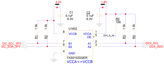
I am using the TXS0102 as a level translator between 1.8V and 3.3V for an I2C bus. There are external pull-up resistors configured as shown in the picture below. On the 1.8V side, I have 10 devices connected, whereas on the 3.3V side, there is only one device.

When I disable the TXS0102 by pulling the OE pin low, all 10 devices on the 1.8V side communicate properly. However, if I keep the TXS0102 enabled as shown below, the bus is pulled low and communication fails.

By removing the external pull-up resistors R1 and R2 on the 3.3V side, devices on both the 1.8V and 3.3V sides work properly. It seems that the sink capacity of the one-shot on TXS0102 is limited, which is causing the issue, although the datasheet does not provide any information about this. Could you explain the reason for this behavior?

Thanks,

Reza 

  • Hi Reza,

    Our engineer who supports these devices is out of office. He will be back Monday. 

    In the mean time, I looked at TXS0102 datasheet - this device only has one-shot accelerators towards VCC. This is a passFET based level translator, and does not re-drive the bus in a sense that it does not re-drive a LOW or HIGH signal to its output. There is no way that TXS0102 itself can pull the bus LOW. 

    When the device is enabled and causes an issue in the I2C data stream, one thing I can think of is the combined PU resistance of both sides of the TXS0102 + the internal 10k PU resistors inside the device push VOL too large. Since it is a passFET based level translator, R1 appears in parallel with R3, same with R2 || R4. This also means capacitance appears in parallel, also keep in mind the internal 10k PU resistors. 

    There is no need to include R1/R2/R3/R4 unless your rise-time is too long. Is that possible with this application? 

    Is SDA getting stuck, or is it not recognized as a valid logic LOW to the 1.8V devices on the bus? 

    Regards,

    Tyler

  • Hi Tyler,

    As I mentioned in my initial message, removing the R1/R2 pull-ups on the 3.3V side resolved the I2C communication issue, thanks again for confirming the root cause.

    I have another question regarding the circuit shown below. Because of some back-feeding issues, I need to sepaarte the power rails on two separate I2C buses. Pull-up resistors are located on Group_1 (left side), which connects to about 6 devices. Group_2 (right side) also has around 6 devices. The power sequence is such that VREG_1P8_1 comes up first, followed by VREG_1P8_2 after approximately 100 ms. During the stand-by right side may remain fully powered down.

    Q1:

    I’m unable to control the OE (Output Enable) pin of the I2C buffer using a GPIO; instead, it's pulled up to the right-side power rail. The datasheet recommends driving OE with a GPIO and keeping it LOW until VREG_1P8_2 is up and running, in order to keep the right-side I/Os in Hi-Z during power-up. Given my setup, is it acceptable to keep OE tied to the right-side supply rail, considering it might be off during power-up?

    Q2:

    Is the TCA9416 the best choice for this scenario? The I2C bus operates at 1 MHz.

    Thank you!

    Reza 


  • Hi Reza,

    Q1. This is acceptable. The datasheet suggest the practice of driving it low until VCC is fully ramped up if the customer is concerned about the state of the I/Os. If you do not care about the state of the I/Os upon bootup, the OE pin can be tied directly to VCCA with no concerns. 

    Q2. TCA9416 is appropriate to use here.