This thread has been locked.

If you have a related question, please click the "Ask a related question" button in the top right corner. The newly created question will be automatically linked to this question.

TXS0102: Pull up and push pull performance

Part Number: TXS0102
Other Parts Discussed in Thread: LSF0002, LSF0102

Hi Team, 


I have few questions about TXS0102DQMR: 

1. Does this device operate in open-drain or push-pull mode depending on whether there is an external pull-up resistor? And since the device itself has a pull-up, how is this determined?

2. During our debugging, we found that when there is an external pull-up on the A side, the rise time can be improved to within 2ns, but when the external pull-up on the A side is removed, the rise time can reach 60ns, though the B output remains around 10ns.

We have confirmed that there is no pull-up on the B output. Currently, the B side output rise time does not meet the I2C fast mode requirement. We tried adding a capacitor, but the signal waveform was not very good. Is there any possibility for improvement?

3. Is the reason the B side output rise edge does not meet requirements because this device has an edge accelerator? How does TI view the I2C fast mode requirement that TR should be greater than 20ns? 

  • Hello Kailun,

    1. Does this device operate in open-drain or push-pull mode depending on whether there is an external pull-up resistor? And since the device itself has a pull-up, how is this determined?

    The device's outputs are open drain as the architecture of this level shifter is FET based. For push pull signals, a higher data rate is achieved because of the active PMOS driver of the input signal. If open drain only, then the data rate is slower due to the slower input edges (the device will not know whether the input is push-pull or open drain, it leverages a switch architecture that opens/ closes depending on the voltage at the input side). 

    2. During our debugging, we found that when there is an external pull-up on the A side, the rise time can be improved to within 2ns, but when the external pull-up on the A side is removed, the rise time can reach 60ns, though the B output remains around 10ns.

    The concern with using external pullups will result in higher VOL levels, see https://www.ti.com/lit/an/scea056/scea056.pdf?ts=1763586668137

    We have confirmed that there is no pull-up on the B output. Currently, the B side output rise time does not meet the I2C fast mode requirement. We tried adding a capacitor, but the signal waveform was not very good. Is there any possibility for improvement?

    In what way? Is the observed rise time below the minimum or greater then the max of 200ns tr for I2C FM mode? 

    3. Is the reason the B side output rise edge does not meet requirements because this device has an edge accelerator? How does TI view the I2C fast mode requirement that TR should be greater than 20ns? 

    The edge accelerator helps the transition edge here. Can you provide more detail on the concern of the observed rise time here. 

    Regards,

    Jack 

  • Hi Jack, 

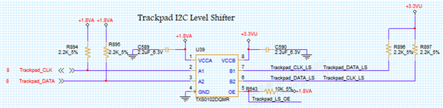
    Thanks for your response! The application circuit and test results summary show as below picture. You can found more detial from the attachment that is the measurement picture.

     https://e2e.ti.com/cfs-file/__key/communityserver-discussions-components-files/151/_0526004E2C8205265F00_N15QA2-TP-I2C-1120.7z

         Question 1: The B side (output side for SCL) TR keep at below 2ns not effact by A side TR (output side for SCL) . Does it effact by TXS0102DQMR about Edge rate accelerator  function?

         Question 2: The I2C Fast mode user guide requiremed the TR rang is 20ns to 300ns. The input side meet the requirement, but B side (output side for SCL)  out put not meet. 

  • Hi Kailun,

    Can you confirm if there is any communication errors that the customer observes? From what it appears, I do not see any concerns that the min rise time can effect the I2C signaling- you may observe some higher % overshoots that can be resolved by using dampening resistors on the output on B-side to achieve slower TR, though it would not impact communication. It is suggested to remove external pullups on A/B side here to not contend with the internal 10kohm pullups however.

    Regards,

    Jack

  • Hi Jack, 

        We have tried some values dampening resistor at B-Side to achieve slower TR, but the dampening resistor must be more than 1k value.

        We think the 1k resistor is not safe to I2C bus. 

        So did you have another ideas to achieve slower TR?

  • Hi Kailun,

     Adding small lumped capacitance (i.e 40pF) at the outputs would also allow for slower TR. 

    Regards,

    Jack

  • Hi Jack, 

         Maybe 40pF is not enough. We can found some information about Edge rate accelerator feature in spec and I have caputured the picture as below. 

         If the Edge rate accelerator enable, the pullup resistor will be chage from 10k to 50ohm. 

         We want TR meet above 20ns, the capacitance maybe closed 400pf, but the 400pf is I2C fast mode max valure. 

         So RC valure need to try and maybe it will affect another parameters.

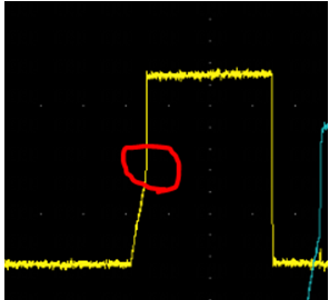
      BTW,  If we remove pullup resistor at A/B side or add capacitance , there will be a clear inflection point from low to high share as below picture.

      The capacitance valure is larger, the inflection point is more clear. 

      We have tried to add capacitance before, but we think the capacitance value and the waveform is not good.

  • Hi Kailun,

    The area circled in red should not be a concern as the signal does not dip back into the VIL max threshold, so communication should not be effected.

    If customer insists on having slower transition times, they can also evaluate the LSF0102/ LSF0002. Both of these LSF devices do not use the edge rate accelerator circuitry so the output rise time is dependent on the external pullup/ capacitive load. 

    Regards,

    Jack