This thread has been locked.

If you have a related question, please click the "Ask a related question" button in the top right corner. The newly created question will be automatically linked to this question.

SN74LVTH16244A: Offset at Buffer Output

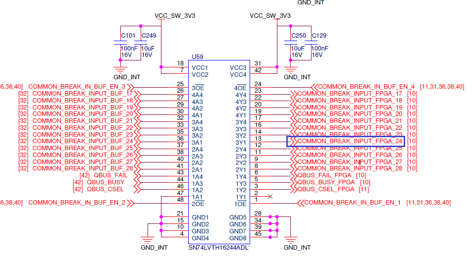
Part Number: SN74LVTH16244A

Hi, I use SN74LVTH16244ADL buffer in my board. This buffer is used between External connector and FPGA. It is observed that one particular output of this buffer is having an output (3Y1) offset of 1V. 

All the outputs are directly connected Artix 7 FPGA, and all signals have same design scheme.

The same issue was observed in different boards. Help me resolve this issue ASAP.

image.png

  • Hi Athulijth,

    Can you make sure that "COMMON_BREAK_INPUT_FPGA_24" is actually configured as an input on the FPGA, and not as an output? Probably your FPGA is introducing bus contention and trying to drive this signal high when the buffer is driving it low, or vice-versa.

    Best,

    Malcolm

  • We checked this in the beginning stage itself and made sure all "COMMON_BREAK_INPUT_FPGA_" signals are  defined as input. We have checked 4 boards, in that 2 boards we had this observation. 

  • Hi Athulijth,

    Have you done an ABA swap between the 2 boards that are working and the 2 boards that have the observation?

    Best,

    Malcolm

  • No, I replaced it with fresh IC and the offset created at the Output of buffer ("COMMON_BREAK_INPUT_FPGA_24 gone.

    One more observation with the same board. 

    COMMON_BREAK_INPUT_BUF_25, after feeding 2.9 V at the input, for this specific line the input was observed to be 1.5V, but for all the other inputs it was about 1.62. And the output from buffer was not coming for "25". 

    Below is the input scheme and it is same for all common break inputs.

    And this observation happened in 1 out of 4 boards. The observation was same even after changing the buffer.

  • Hi Athuljith,

    Probably the issue is the 10nF capacitor you have on the input. Please note this device's input rise and fall time requirements:

    With your low-pass filter values of 1k ohms and 10nF, you can expect your input to have a slew rate of about 0.1V/us, which correlates with an inverse slew rate of 10,000ns/V. This is much slower than the requirement of 10ns/V or faster.

    With an input signal this slow, you can expect to damage the input buffer, output buffer, or potentially the whole device from repeated oscillations during signal transition.

    Also, why are you giving a 1.5-1.62V input to this device for all of the inputs? The input level high voltage is 2V. Either every input stage has been damaged to some degree by the slow rise time from the low-pass filter, and the damaged input buffer stages are preventing the input from fully rising to 3.3V, or some resistor divider or something else on your board is causing you to explicitly not meet the correct input voltage level requirements for this device.

    1.5V to 1.62V is right around the input transition threshold of this device at 3.3V VCC, and you can expect the outputs to oscillate between 3.3V and GND if the input voltage is maintained at this level, instead of rising above 2V as demanded by the datasheet.

    Best,

    Malcolm