This thread has been locked.

If you have a related question, please click the "Ask a related question" button in the top right corner. The newly created question will be automatically linked to this question.

TXS0108E-Q1: TXS0108E output

Part Number: TXS0108E-Q1
Other Parts Discussed in Thread: TXS0108E

Hello TI experts,

It's a special design with TXS0108E.

The circuit is simplified as below.

If SoC_A output low on Port A of TXS0108E while SoC_A output high on Port A of TXS0108E, what will happen?

Will this case lead to over current on GPIO of SOC_A or SOC_B?

Thanks a lot.
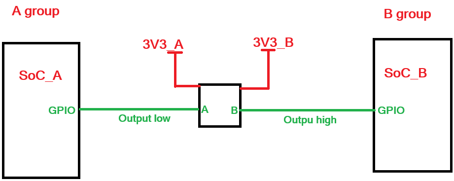
image.png

  • Hi Huan,

     What is the direction of the signal flow? If the application is A-> B or B->A, the respective output will be driven low as well. By default, if nothing is driving the IOs, the state of the A/B ports will be logic high due to the internal pullups (assuming the device is enabled during this time). 

    However A and B should not be driving into each other especially with opposing logic as this will cause bus contention concerns.

    Regards,

    Jack 

  • Hello Jack,

    During normal mode, one port is configured as input while another is configured as output, there is no issue

    We are considering a failure case that both ports are configured as output.

    So, how to design to protect?

    Thanks a lot.

  • When at least one of the A/B inputs is low, then the TXS works as an analog switch, i.e., there is a direct connection (with about 300 Ω) between the A and B pins. So when both GPIO pins are outputs with different voltages, this can lead to overcurrent on both GPIO pins.

    If you want to prevent damage in this case, you have to insert current-limiting resistors.

  • Hello Clemens Ladisch,

    Here are two failure cases as shown below:

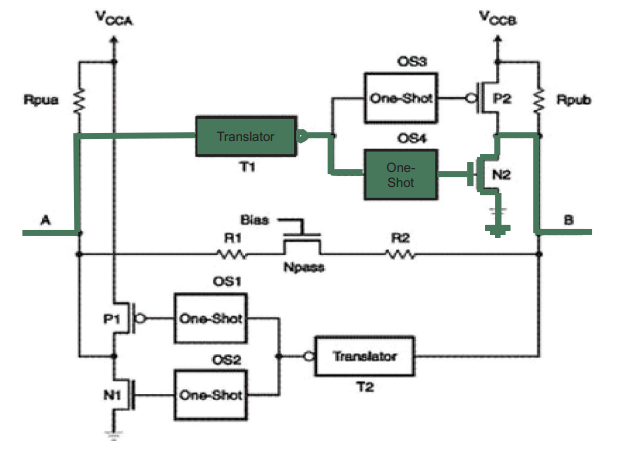
    And I think the output low path of TXS0108E from A to B and from B to A are different.

    TXS0108E Port A output low and transfer to Port B as below marked in green:

    TXS0108E Port B output low and transfer to Port A as below marked in red:

    Is that right?

    If limit current of Soc GPIO output is 100mA, whether only add series 33ohm in Port B enough? See below:

  • Hi Huan,

    100mA through the device will result in damage. The continuous max output current through the IO channels is rated for 50mA. However, you should still check with SoC on A/B side if this current can be accepted downstream as well. 

    Regards,

    Jack

  • The one-shots (green) are active only for a few nanoseconds, when a rising or falling edge on the other side is detected.

    For the DC current limit, you need to look only at the (red) path through the switch. Note that it is bidirectional (the pass transistor has no difference between source and drain). According to the voltage drop shown in the datasheet, R1+R2 is typically 300 Ω.