TXB0108: Level shifter not functioning

Part Number: TXB0108

Hello team,

We are using TXB0108 level shifter in our application inbetween CPLD and D type flip flop.The CLD is operating at 3.3V logic and D type level shifter operating at 5V logic .The signal we are expecting is bidirectional.The level shifter scheamtic is attached here. The level shifter is cnnected in the followign way.

Vcca=3.3,OE=3.3 and Vccb =5V

image.png

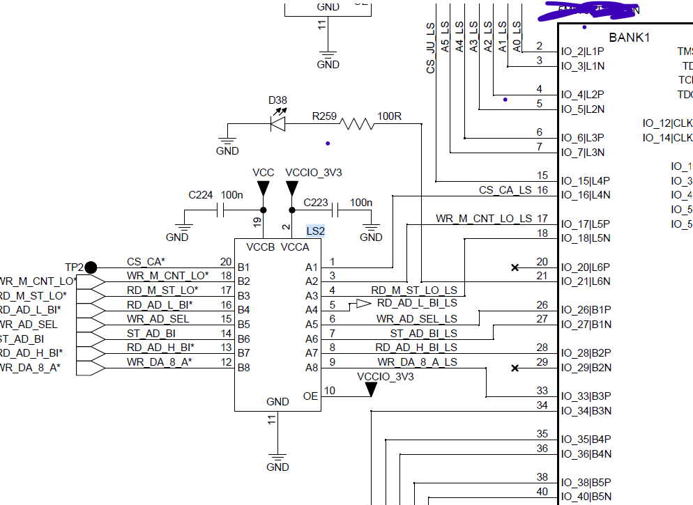
During testing we found that the level shifter is continously giving zero output even though we change the inout signal .we would like to hear from you what could be the potential cause of this problem?Does this level shfter require any power on delay for the OE pin ?

Regards,

Letheesh G

  • Flip-flop control signals are not bidirectional. The schematic does not show the flip-flop.

    Show an oscilloscope trace of the relevant signals at both sides of the TXB.

  • Hello Ladisch,

    The data sheet mentioned in the following way.

    ...

    I would like to seek clarification on the recommended connection of the OE (Output Enable) pin for the TXB0108 level shifter during power‑up.

    In our design, the TXB0108 is used in the following configurations:

    1. CPLD (3.3 V) → Flip‑Flop (5 V):
      In this case, the level shifter acts as an input on the A‑side, accepting 3.3 V signals from the CPLD and translating them to the 5 V domain.

    2. Bidirectional Signal Translation:
      The level shifter also interfaces with other peripherals, where it accepts input signals from the 5 V side and translates them to 3.3 V. Hence, the device is used in a bidirectional manner depending on the signal direction.

    Both 3.3 V (VCCA) and 5 V (VCCB) supplies for the level shifter are generated on the same PCBA and are powered up together.

    Given the above usage scenarios, could you please confirm:

    • Whether it is necessary to connect the OE pin to GND through a pull‑down resistor to ensure the device remains in a high‑impedance state during power‑up?
    • Or whether directly tying OE to VCCA is acceptable, considering both supply rails are generated on the same board?

    Regards,

    letheesh G

  • Hi Letheesh,

    Whether it is necessary to connect the OE pin to GND through a pull‑down resistor to ensure the device remains in a high‑impedance state during power‑up?

    This is only needed if customer wishes to have the I/Os in HIGH-Z state during power up. If customer does not care about the status of the I/Os during this time, it can be tied directly to VCCA with no concerns. Do you have any update from the suggestion provided by Clemens? 

    Regards,

    Jack

  • Thank you jack for clarifying the same   .

    Can you please provide me the the  Revision J of the data sheet (TXB0108) ?

    Regards,

    Letheesh