This thread has been locked.

If you have a related question, please click the "Ask a related question" button in the top right corner. The newly created question will be automatically linked to this question.

LSF0204: Use LSF0204 for I2C + GPIO

Part Number: LSF0204

Dear Team,


we would like to use LSF0204 for:

-> I2C (400kHz)  translation from 3.3V ( Master) to 1.8V (slave)

-> Gpio translation from 3.3V to 1.8V 


1) We only use 3 channelc, can we connect booth A and B Side of fourth channel to GND?

2) We will connect Vref_B to 3.3V and Vref_A to 1.8V  and have 100nF on Vref_a and 100nF on Vref_B. is it ok?

3) We will connect EN to Vref_A -> 1.8V as the 1.8V is generated with LDO from 3.3V is it ok?

4) How to size the pull-up for the I2C 400kHz -> 

SDA(SCL on the A site
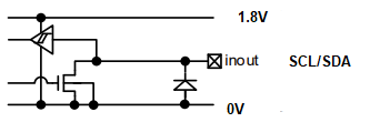
image.png

For the B site ( 3.3V) Rpullup 1kOhm?

For the A site (1.8V)  Rpullup 464Ohm?

Or can we also have larger resistors? 

5) Regarding the reistor for the GPIO we also need pull-ups , how to size them?

the GPIO input is as below
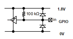
image.png


Best Regards,

d.

  • 1. Unused channels can be left open, or pulled up to the supply.

    2. Vref_A/B are not supply pins but bias voltage pins. Capacitors are not as important as with digital devices, but do not hurt.

    3. Yes.

    4. The LSF is a passive switch; for low signals, both sides are connected, so the two pull-up resistors act in parallel. The I²C specification limits the total pull-up current to 3 mA in most cases, so I'd recommend 2.7 kΩ on the 3.3 V side and 1.5 kΩ on the 1.8 V side (assuming there are no other pull-ups on the bus). Check that the 1.8 V devices do not have a lower drive strength.

    5. This depends on how slow the signal edges are allowed to be. The pull-up resistor and the capacitances form a low-pass RC filter. (Estimates for the capacitances are 10 pF per device and 1 pF per cm of trace.)

  • Hello,

    1, Yes, if the 4th channel is not used, it is acceptable to connect both A-side and B-side of that unused channel to GND. No pull-up resistor is required for the unused channel.

    2, It should be OK. A-side should be the lower-voltage side, and B-side should be the higher-voltage side. 100 nF decoupling capacitors on VREF_A and VREF_B are also fine and should be placed close to the device.

    3, For LSF0204, EN is referenced to VREF_A and is active high, so tying EN to VREF_A = 1.8 V is OK for an always-enabled application. Since the 1.8 V rail is generated from the 3.3 V rail through an LDO, this should be fine.

    4, For I2C, pull-ups are required on both SDA and SCL on both voltage sides because I2C is open-drain. The final value depends mainly on bus capacitance and the sink-current capability of the I2C devices. For 400 kHz Fast-mode I2C, the pull-up resistor should satisfy the rise-time requirement:

    See the related application note : I2C Bus Pull-Up Resistor Calculation

    The values you use in B-side 1 kΩ and A-side 464 Ω are quite strong for I2C. When the bus is pulled low, the device pulling low may need to sink current from both pull-ups. With 1 kΩ to 3.3 V and 464 Ω to 1.8 V, the total low-level current can be around 6 ~ 7 mA, which are quite high for I2C devices. Therefore, I recommend using larger resistors first, such as 2.2 kΩ, and then verifying SDA/SCL rise time and VOL on the oscilloscope.

    5, The internal 100ku pull-up @ GPIO input is a little large, it may cause a slow rising edge if the load capacitance is not small. For normal GPIO speed, a typical external pull-up would be required. Please also refer to application note : I2C Bus Pull-Up Resistor Calculation for do the estimation. 

    Regards

    Brian

  • Dear Support,

    thank you for replay.

    1) So the 100nF decoupling caps are not mandatory and we can remove them is we don't have space?

    2) I have in the system 2k61 and 1k, i think i will use 2k61 on 3.3V and 1k on 1.8V, is it ok? ( there are no other pull-ups )

    3) For gpio i will use 10k on 3.3V side and 10k on 1.8V side

    4) regrading RGY package, We can GND or left floating pins 5,10,6,9? 5 and 10 is ch4 not used, and 6 and 9 and NC pins.

    Also the thermal pad on RGY package can be connected to GND?

    Br,

    d.

  • 1. The currents through the pull-up resistors will load the supplies, so there should be decoupling capacitors somewhere.

    2. Sounds OK.

    4. NC pins should not be connected. Pins 5 and 10 do not matter and can be left open; if you connect them to different voltages, a current can flow.

    The thermal pad can be left floating or grounded; see [FAQ] Where do I connect the thermal pad of the logic QFN devices?

  • 1, 0.1 µF is a recommendation and place it close to the VCC/reference pins to reduce rail noise and voltage droop during transitions.

    2, This is generally OK for LSF0204, assuming the devices driving LOW can sink the current. 

    4, Pin 5 / pin 10, unused CH4 A4/B4 and Pin 6 / Pin 9 NC are ok to leave floating / no connect. 

    Yes, the exposed thermal pad can be connected to the PCB GND copper/plane. The datasheet mentions the RGY package thermal pad must be soldered to the PCB for thermal and mechanical performance

    Regards

    Brian