This thread has been locked.

If you have a related question, please click the "Ask a related question" button in the top right corner. The newly created question will be automatically linked to this question.

SN74LVC8T245PWR-POWERUP SEQUENCE

Dear All,

Good Day, I am using SN74LVC8T245PWR as a level translator from the 2.5V to 3.3V.VCCA=2.5V and VCCB=3.3V. Pullup resistors are provided for some signals, this pullup is powered from aux supply. As per my design my powerup sequence is VCC _AUX, 3.3V & 2.5V. Kindly let me know that

1. what is the powerup sequence of this leveltranslator ?

2. whether this pullup supply will affect my 3.3V or 2.5V supply through leveltranslator during power up?

Regards,

Rajesh.S

  • Hi, Rajesh,

    here is the feedback for you. any further thing, please let me know.

    1. what is the powerup sequence of this leveltranslator ?

    [Junjie] there is no power sequence  requirement for this part.

    2. whether this pullup supply will affect my 3.3V or 2.5V supply through leveltranslator during power up?

    [Junjie] could you please share with us you schematic and what voltage of your Vcc_aux is? I will check your design and then provide you the feedback.

    BR
    junjie


  • Dear Sir,

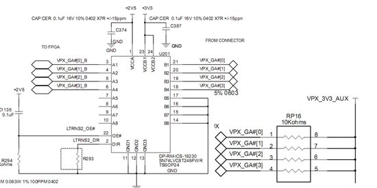
    Kindly find my schematics .

  • Hi, Rajesh,

    I can not find the attachment, did you miss it?

    BR
    junjie

  • HI,

    Sorry for the inconvenience, I added as a image.

  •  

    Rajesh,

    since your AUX is 3.3V, the same with VccB side, it should be no problem in normal operation.

    but when power up, suggest make the DIR is low to set the B side are input, not output in case some current from 3V3_AUX to +3V3 since +3V3 is not reach up to 3.3V.

    BR
    junjie


  • Hi,

    I was not getting clear, can you elaborate the same.

    Rajesh.S

  • Rajesh,

    What I said is for two scenarios. one is for normal operation after power up, the other is power up.

    1. For normal operation after power up, at the output side, we don't recommend to add the pull up the resistor to a higher power supply than output VCC. for your applicaiton, the VccB is 3.3V, and the pull up resistor is connectted to another 3.3V. since they are all 3.3V, your design should be OK.

    2. For power up scenario, since your AUX 3.3V  is on firslty, when the VCCB 3.3V is power up, if the DIR is high which means the translation is from A to B, B is output side , so their will have the situation that VccB is lower than the AUX which is connectted to the pull up resistor. that will have the chance to cause the inverse current from AUX to the VccB.  so in your schematic, for signal LTRNS2_DR, if you have the contorl for it, I suggest to contorl it to be low voltage when power up. if no contorl for it, since you have connectted it to GND, that will be OK.  as you know when DIR is low, the translation is from B to A, the B side is input, not output.

    any unclear, please let me know.

    BR
    Junjie

  • Hi,

    Thanks for the information, now it is clear.

    Rajesh.S