This thread has been locked.

If you have a related question, please click the "Ask a related question" button in the top right corner. The newly created question will be automatically linked to this question.

Driving issue with TXB0106

Other Parts Discussed in Thread: TXB0106

Hi,

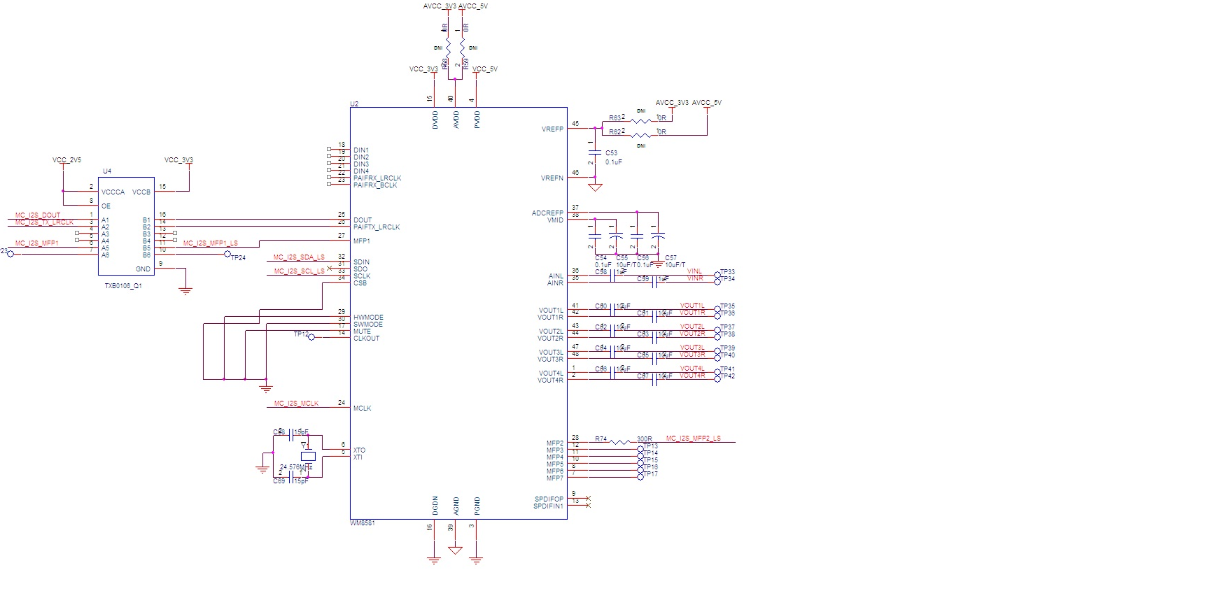
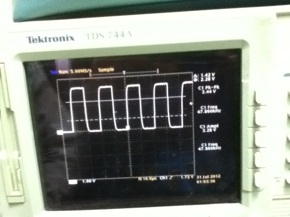
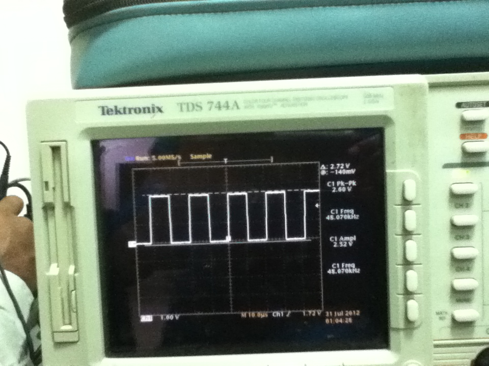
We are using TXB0106(TSSOP package TXB0106IPWRQ1 ) for level shfting of signals between FPGA(2.5V)  and Audio CODEC(3.3V). We could see level shifting operation happening properly for low frequecies which are around 48KHz. But level shfting is not happening properly for signals of 3MHz frequency. The input to the level shfter is perfect square wave of 3MHz frequency(low level at 0V and high level at 2.5V). At the output of the level shfter we are expecting perfect square wave of 3MHz frequency(low level at 0V and high level at 3.3V). But this is not happening. The output signal frequency is coming 3MHz but it is not square wave. Signal level is slowly rising and slowly falling similar to ramp. The signal swing is between 0.68V and 2.5V against the expected 0V and 3.3V. Due to this issue CODEC is not able to detect the signals properly. We are connecting VCCA to 2.5V with 0.1uF decap and VCCB to 3.3V with 0.1uF decap.  We have tried by increasing the FPGA drive current from 12mA to 16mA but still we could not see any improvement. Please help us to resolve this issue.

Regards,

Narayana Rao


  • Hi, Narayana,

    For  TXB0106, it should be work at 3MHz with VccA is 2.5V and VccB is 3.3V.

    Maybe two things nee to be checked in your design when 3MHz signal input.

    1. The TXB0106 is target for driving high impedance load, it doesn't have high current driving capability.  Only about 20uA, you can check the datasheet for Vol and Voh. so please check with the Audio codec vendor, when driving it, how much current will be sourced from or sunk into the driver.

    2. when 3Mhz signal input, is there any internal or external pull up or pull down resistor at the Audio Codec side?

    If rule out above causes, could you please send me your schematic and the waveform you got, and then I will deep into it and see the details.

    BR

    Junjie 


  • Junie,

    Thanks for quick response. In the mode we are testing we are driving level TXB0106 input(A side) with 3MHz  signal from FPGA (signal swing between 0V to 2.5V). we want to connect TXB0106 output(B side 3.3V) to CODEC. But when we observed improper signal at TXB0106 output(B side) we suspected the loading effect of CODEC on TXB0106 and we have disconnected CODEC from the output of TXB0106(means there is no load the output of TXB0106). But still we are getting improper signal at TX0106 output as I mentioned in my earlier post. That is the reason I am not suspecting the loading effect on TXB0106 output. There are internal or external pull up or pull down resistor at Audio CODEC side.

    If you still need wave form and schematic I will paste in my next reply.

    Thanks,

    Narayana Rao


  • Junie,

    Please have a look at the waveform we are getting at TXB0106 output. We are feeding perfect square wave of 3MHz at input. We are using CODEC WM8581.

    When we feed 48KHz signal to TXB0106 we are getting Square wave at the output.

    Regards,

    Narayana Rao


  • Hi, Narayana,

    Is this waveform got when no loading on the TXB0106? seems the one-shot circuit is not opened.

    Could you please share with me the schematic? both input and output waveform at 3MHz and 48Khz when no any load at TXB0106?

    Also, is this the signal case or mutiple cases?

    BR
    Junjie

  • Junjie,

    We got this waveform when WM8581 CODEC is connected. But we have observed same waveform in no load condition also. It doesn't matter whether we connect load or not, we are getting similar wave form when 3MHZ signal is fed. But when we feed 48KHz signal we are observing square wave signal at the output in both no load case and when CODEC is connected. I am inserting the schematic below. U4 is TXB0106 IC and U2 is WM8581 CODEC. We are feeding 3MHz signal to TXB0106 6th pin(In schematic MC_I2S_MFP1). We are monitoring output at TXB0106 11th pin (In schematic MC_I2S_MFP1_LS). We are feeding 48KHz to TXB0106 3rd pin(In schematic MC_I2S_TXLRCLK) and we are monitoring 48KHZ output at TXB0106 14th pin. This issue is observed in 2 boards we mounted and we also tried by replacing TXB0106 with another part but observed same behaviour.

    Regards,

    Narayana Rao


  • Hi, Narayana

    Could you please also provide me both the input and output waveform at 3MHz and 48Khz application?

    BR
    junjie

  • Junjie,

    Please find waveforms below.

    Regards,

    Narayana Rao


    48KHz input wave form:

    48KHz output waveform:


    3MHz input wave form:

    3MHz output waveform:


  • 48khz input wave form is attached above. Some how this waveform is missed in above replies.

    Regards,

    Narayana Rao


  • Hi, Narayana,

    Based on your schematic, input and output waveform, we think the capacitive load at the 11th pin (In schematic MC_I2S_MFP1_LS) is very large which caused the signal can not reach up to the 3.3V or down to 0V when one shot is on.

    if you confirm only have one receiver and you have had remove the recevier, but you still have the same waveform, I suspect your trace maybe very long which cause the larger capacitance. so please check the length of the PCB trace. I saw you have some floating pins, can you short 6th pin to 5th pin and then check the output of 12th.

    BR

    Junjie

  • Junjie,

    As suggested by you, We have shorted 6th pin and 7th pin(TP23 which is floating) and checked the output at 10th pin which is floating(TP24) and not connected to any load or PCB trace. Still we are not getting Square wave at the output(similar waveform mentioned earlier is observed). I confirm you that we have lifted the output pin of TXB0106 from PCB and then we observed same waveform(which is not square wave) on probing on the output pin on the TXB0106. This is the reason we are not suspecting load issue/PCB trace issue. It will be great if you have TXB0106 with you and check by feeding 3MHz (0 to 2.5V) at TXB0106 input  and observe the signal at the output(Supply:VCCA 2.5V, VCCB 3.3V).

    Please let us know if you need any more inputs from me.

    Regards,

    Narayana Rao


  • Hi, Narayana,

    Yes, I can get the samples to do the checking. it will take some time for me to get the samples, any update, will let you know. but this part has been released several years, no this kind of issue happened if the part is OK.

    For your issue, based on the waveform your provided, we are very sure it is caused by the larger capacitance. Not sure why you got so strange thing. please make sure below things.

    1. The input signal has enough current drive capability. if drive two channels at the same time, at least 4mA need.

    2. Make sure the not so large capacitance loading.  your wavefrom looks you have larger capacitive load even in the 48KHz output, have you measured the length of PCB trace, and also check the CIO of the recevier?  Please evaluate them and make sure they are not very large.

    3. Seems there is no serial resistor between TXB0106 and your receiver, when you tested the output when no any loading, you mean you remove the WM8581 CODEC  from your board?

    4. Does your TP23 and TP24 has so long PCB trace? please make sure they are short enough.

    5. What is your probe capacitive load? please make sure it is lower enough.


    BR
    junjie

  •  

    Junjie,

    As pointed by you correctly in earlier reply, The culprit here is probe capacitance which is around 90pF. I got a probe with 15pF capacitance and now I could see square wave output. Thanks much for your help. You need not get TXB0106 samples since the issue cause is known to us now.

    Regards,

    Narayana Rao


  • Hi, Narayana,

    Thanks for your feedback here. any further thing, please let me know.

    BR

    Junjie