This thread has been locked.

If you have a related question, please click the "Ask a related question" button in the top right corner. The newly created question will be automatically linked to this question.

74HC595 shift register basic questions

Hello all,

Newbie here.

I'm putting together a simple website regarding some basic electronic/logic circuits, and one of the sections is on shift registers.
(I'm not an engineer, just an old hobbiest dating back to the S100 bus)

For teaching (and learning for me) purposes I've put together a simple circuit (chip, connectors, resistors and LEDs), built it, and interfaced it to an Arduino.
The site includes a series of programs that demonstrate, very simply, how shift registers work, and what you can do with them.

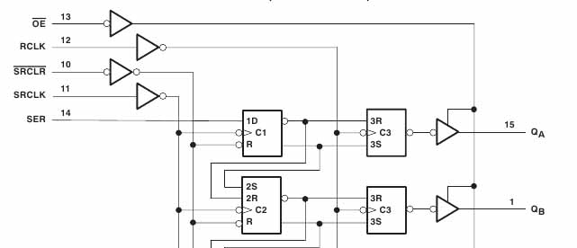
I would like the explanations to be as accurate as possible, so I'm going over every detail. The Texas Instruments datasheet on the 74HC595 is the best datasheet out there because of the logic diagram - the workings are VERY clear (my thanks to the people who wrote the datasheet).
But there is one part of the datasheet that is confusing me, thus my presence here.

Long-winded introduction, now to the two questions:

1. The data sheet states that the storage clock is a "D-type storage register". I'm assuming that it means "based on a D-type flip-flop".
Here is the relevant section of the datasheet:

But the Wiki explanation of flip-flops gives a slightly different appearance for a D-flip-flop -
One data input, one clock, one each of set/reset, and Q and Q complement.
Am I right that when it says "D-type storage register" that it means "based on D-type flip-flops"?
Does the appearance (number of connected leads) of the flip-flop matter?
 Or do the workings (logic table) of the flip-flop determine its name?

2. I can't find anything in the datasheet regarding the type of flip-flop that is used in the first level shift register.
Based on its leads, it seems like it would be a classic "D-type" flip flop. Is that right? Or is it another type?

In advance, I thank anyone who would wade through my verbose questions.
Tim


  • At its very basic configuration, a D flip flop has a data input D, an output Q and a clock. Additional optional pins are set, reset and not Q.

    I must tell you that the device you are commenting confused me, since it seems to be that the output of the first flip flop is sent, not to the Q input of the next one, but to the SET input of the next one (and the inverted output to the reset input). So it is not the traditional implementation of chaining data out Q to next data in D. Additionally, it has two independent clocks, one for shifting, one for storage.

    Did you check other registers, like the CD4094? Its datasheet if more old fashioned, but it has the Q-D-Q-D chaining, and latches for data storage.

  • Thanks very much for your response!

    I chose the 595 only because I had some for another project.

    But the CD4094 that you mention looks very nice and much more understandable - the logic diagram is far more "traditional" as you mention.

    So I guess a flip-flop is not necessarily defined by its pinout, but rather by its "function" or logic table.

    I'll order some of the CD4094s and play with them a bit. I may change the page to focus on them instead.


    Again, thanks very much for your excellent answer!

    Tim


    PS - I love your Feynman avatar!

  • I have read many books from Feynman, the guy was really special, a brilliant physicist but also a person that loved to teach to everyone, and was also curious about so many human activities. Definetly not the "scientist on an ivory tower" type. 

    Regarding the FF I agree with you, basically a FF is defined by its functionality.

    You are welcome, may you have success with your projects and website.