This thread has been locked.

If you have a related question, please click the "Ask a related question" button in the top right corner. The newly created question will be automatically linked to this question.

SPI Expander using SN74LV595A

Other Parts Discussed in Thread: SN74LV595A

I am using an SN74LV595A as an SPI output expander as many folks do. I would like to cascade two or more devices to allow for more than 8 output bits with a single SPI chain. There is a timing issue with doing this though.

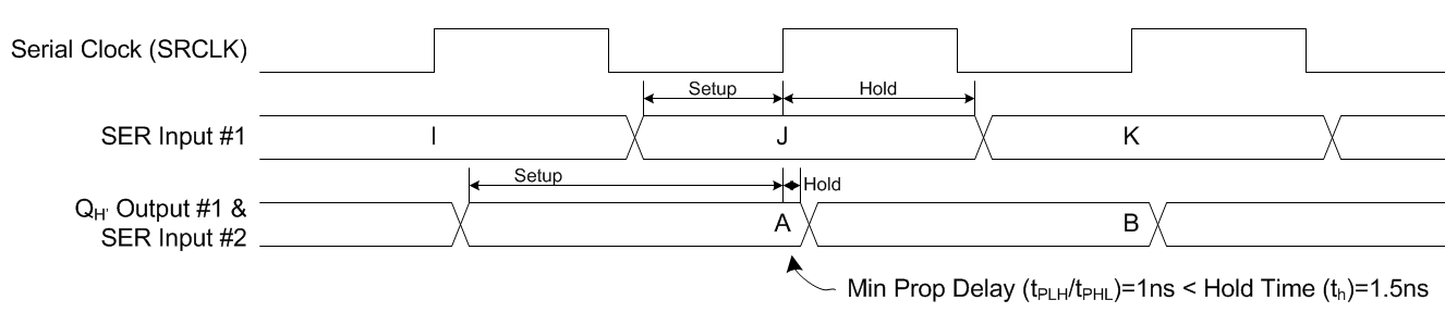
Common usage of an SPI port changes the serial data on the falling edge of the serial clock as would be appropriate to drive the SER input of the SN74LV595A as shown in the timing diagram on page 4. However, the timing of the serial output QH' changes state on the rising edge of SRCLK. This creates an issue with the hold time into a cascaded SN74LV595A. The datasheet gives the 3.3V required hold time as 1.5ns but the minimum propogation delay from SRCLK to QH' is 1ns.

Is there an easy way around this? Are there any similar parts to the SN74LV595A that update QH' on the falling edge of the clock?

Thanks.

  • Dale,

    I think there is just a mix up in terms here.

    You need to remember that there are 2 clocks that affect this device. SRCLK clocks QH' and RCLK clock QA -QH.

    The SRCLK affects the first bank of latches. RCLK affects the second bank of storage registers. The values in the storage registers are not affected by the values at their inputs until the rising edge of RCLK, so clocking in values via SER on the rising edge of SRCLK has no effect on on the values stored in the storage register.

    So if the value of QH' changes on the rising edge of SRCLK, it will not effect the stored value of the first storage register of the cascaded device. It becomes an input to the second cascaded device as SER is to the first.

    So you can clock in 16 values via the SER on the rising edge of SRCLK and they will be sequentially loaded from 1 device into the cascaded device.

    They will only be clocked to the storage register (and the outputs if OE is low) on the rising edge of RCLK.

    I hope that this explains how the SN74LV595A can be cascaded to output multiple bit values.

    Please let me know if you have any additional questions.

    Richard Elmquist


    If you clock in your data with the SRCLK

  • Richard,

    Thanks for the reply. My understanding of how the part works is the same as your description. The issue is a timing problem wrt the published datasheet specifications for minimum prop delay and hold time. Most SPI cascaded devices change their output data on the falling edge of the serial clock to avoid this problem. A cascaded chain can use devices that change their output data on the rising edge of the clock but it requires the minimum prop delay of the preceding device to be larger than the hold time of the subsequent cascaded device.


  • The end of the previous post got chopped. I'll try to repeat it.  (This reply widget sure is slow and buggy.)

    If you look at the diagram above. The SER input #1 uses a typical SPI timing where the data changes shortly after the falling edge of the clock. This provides a generous amount of setup and hold time. The output from the 595A (SER Input #2) which changes on the rising edge still provides a generous amount of setup time but the hold time is very short. Rising edge devices can still be used in a cascaded chain but it requires the minimum prop delay from the preceding device to be more than the hold time required by the subsequent device. For the 595A the minimum prop delay (at 3.3V) is given as 1ns and the required hold time is 1.5ns which means the subsequent device is not guaranteed to receive the serial input data properly. This can be corrected by either using a device similar to the 595A that changes its output data on the falling edge of the clock or by some assurance that the minimum prop delay is actually longer than the hold time for this part. (I suspect this is the case from the length of the typical prop delay given in the datasheet and that this part seems to get used successfully in a cascaded configuration.)

    Thanks for your help in resolving this.

  • Dale,

    There does appear to be an issue in these timing specifications. Realistically the tp is greater than the 1 ns that is specified as the minimum and there is not an issue, but the data sheet numbers do imply that there is a possibility that the tp could be less than the th. Let me check with the factory engineers on this to get their take on this.

    Richard Elmquist

  • Dale,

    The factory engineers stated that the 1ns propagation delay will never happen. 1ns was a standard value that was used with all parts in the past. The engineer stated that in reality the absolute minimum propagation delay would be 7ns - 8ns so there would not be an issue in terms of timing.

    Please let me know if you have any further questions.

    Richard Elmquist

  • Thanks. That will fix our timing analysis. Will you be updating the datasheet with a more realistic value?