This thread has been locked.

If you have a related question, please click the "Ask a related question" button in the top right corner. The newly created question will be automatically linked to this question.

CB3T Data Direction

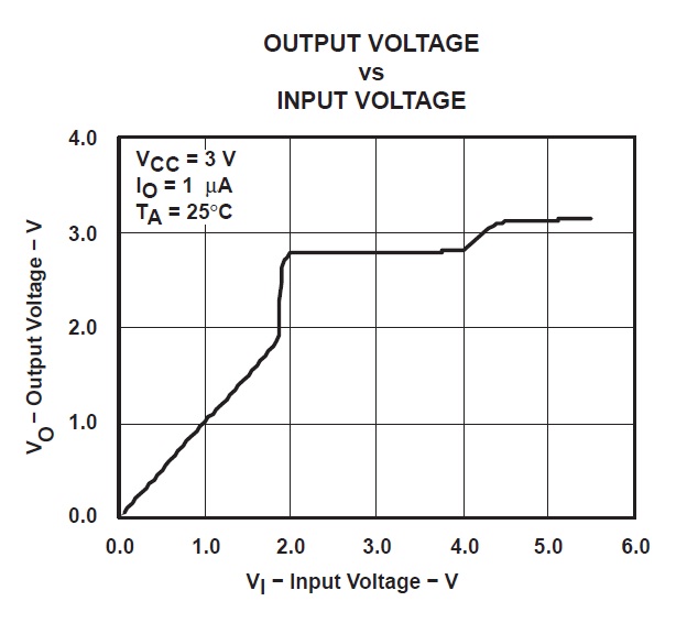
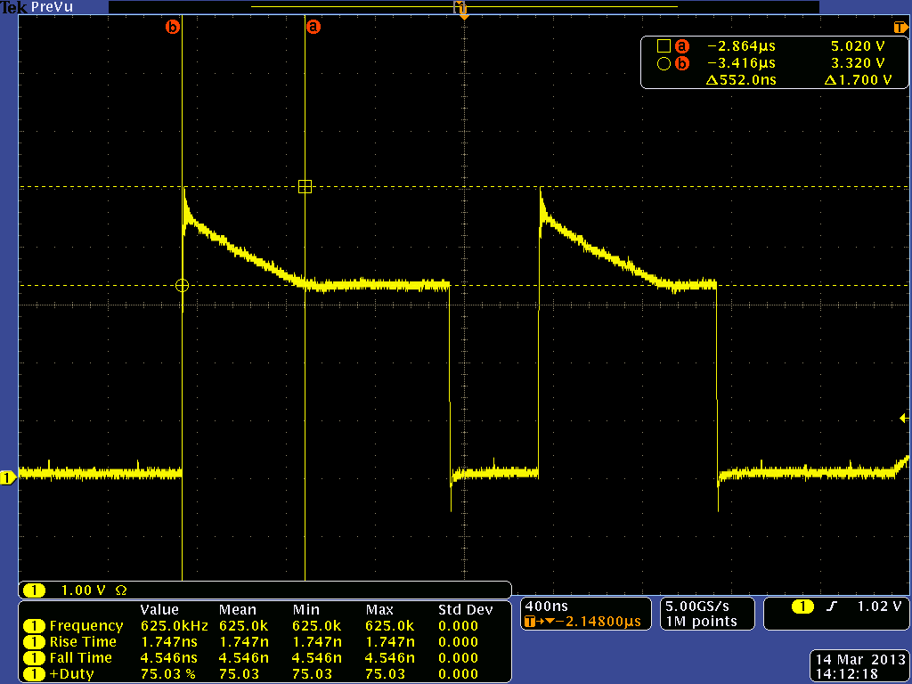
Does CB3T logic provided level translation in either direction?  For example, for a CB3T device with VCC = 3.3V, would a 5V level input to Port A be clamped to 3.3V at Port B, and vice versa (Port B to Port A)?  I'm using a SN74CB3T3384PW device and have a 2.5 MHz, 0-5V clock input to pin 2B1.  The resulting output at pin 2A1, however, has an amplitude of about 4.6V ramping down to 4.0V.  It's clearly not clamping to 3.3V.  Any help with this would be greatly appreciated.

  • CB3T device is a down translator. If VCC is 3.3V and the input is 5V then it should translate down to 3.3V. The input voltage must be 1V above Vcc for it to translate up to VCC.  So this case should work. It will not go back the other direction without a pullup resistor on the high side.

    I am not sure why you are not seeing a 3.3V signal out when the input is 5V. This should work. can you confirm the marking says CB3T?

    The way the part works is it is an N-channel which will output Vcc-1v. The there is an internal pullup type circuit that uses the input signal to pull it up to the Vcc level. That is why the input must be 1V higher than Vcc.

  • Hi Chris,

    Thanks for the reply.  The package marking for the part I'm using is "KS384", which agrees with the 74CB3T3384 datasheet for the TSSOP/PW package.

    I'm assuming that Figure 3.3 (Output vs Input Voltage) of the DS is a graphical version of your description above.  I've included the Figure 3 I/O characteristics for VCC = 3V below.

    Upon further testing I'm seeing that the CB3T3384 does indeed translate 5V to 3.3V, but it ramps very slowly down to 3.3V, on the order of 550 ns!   I've included a scope shot of the output waveform below.     I was assuming that this device is much faster than this, any insights would be appreciated!

    Best Regards,

    Mick

  • This device should run up to 100Mhz. The waveform does not look like a CB3T waform should look.  Is there any other parts that may be affecting the output. It looks like a capacitive discharge.

    This looks like a typical CBTD waveform where a fast edge will cause a charge pump effect. The CB3T devices shoul not do this.

    Have you tried another part to see if this one may have been damaged?


  • Hi Chris,

    I've noticed that another set of clocks through the same 74CB3T3384 package exhibit behavior consistent with Figure 3.3 of the DS (aka proper behavior).   All signals on the 3.3V side of this 3384 go to a Xilinx Spartan 6 FPGA.  I'm suspecting that, for the problem signals described above, the FPGA may be incorrectly programmed as an output instead of an input.   Will continue to investigate. 

    Thanks much for the information you've provided, it's really helped with troubleshooting this issue.

    Thanks,
    Mick

  • I isolated the 74CB3T3384 from the FPGA and the resulting output is much improved.  The logic 1 levels stay below 3.3V.   Our FPGA designer said that the FPGA pin was not configured as an output, but as an input with internal pullup.  It appears that this pullup may have caused the problem.  We will remove the pullup from the FPGA input and re-evaluate.