This thread has been locked.

If you have a related question, please click the "Ask a related question" button in the top right corner. The newly created question will be automatically linked to this question.

SN74LVC8T245PW output pulses when Powerup

Other Parts Discussed in Thread: SN74LVC8T245, LM1117, SN74AVC8T245
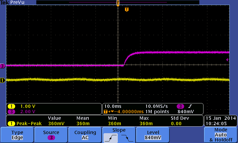
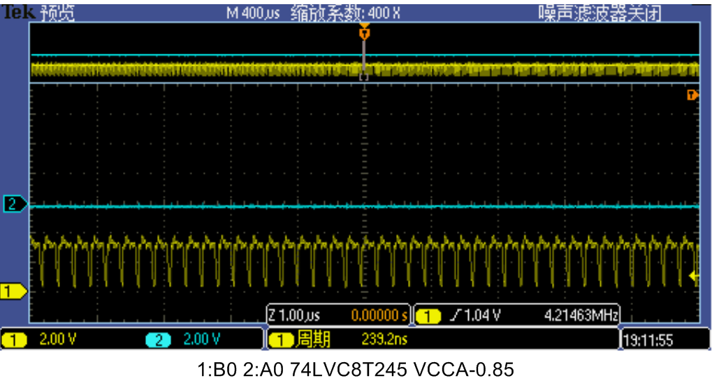
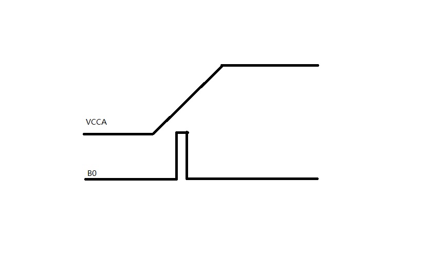
As the image dispalyed, when VCCA was later than VCCB, there was pulses on the B side of SN74LVC8T245.
VCCA is connected to MAX8660, and it is powered on 2s later.VCCB is connnected to LM1117. The power up sequence cannot change.
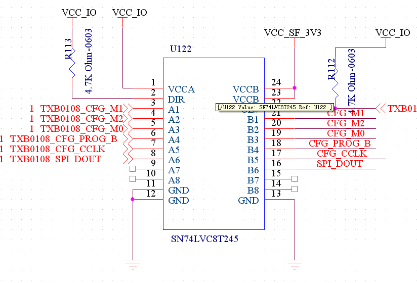
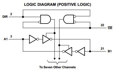
The circuit is very simple, OE and DIR:pulled up with 4.7K Res, A1:conneted to IO of CPU supplied by MAX8660, B1: connected to IO of FPGA supplied by LM1117. On the time voltage of VCCA was up, there was a pulse on the B1(A1 was always low), which affects the status IC on B side.
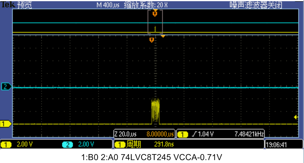
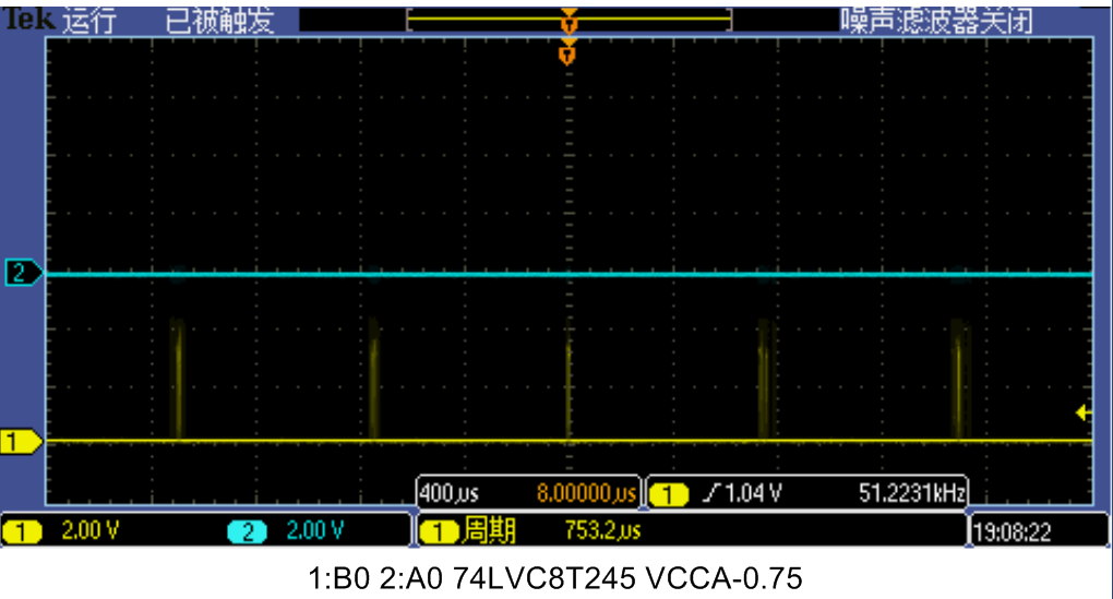
Then i tested the output of B1 when VCCB=3.3V, supplied VCCA with adjust power source. When VCCA change from 0.71V to 0.9V, there is periodic pluses on B1.
I have read the datasheet of SN74LVC8T245, it is made of  OR gates. Is that the reason cause the pulse on output of B?
Using SN74AVC8T245, all signals were right on B side.
I want to get the reason that described above and the method to get rid of it.


  • Hi,

    When OE and DIR are pulled up by 4.7k resistor, SN74LVC8T245 will be at isolation status and both ports are at high Z state.

    I repeated the test with dual port DC supply. The OE and DIR are pulled up by 4.7K resistor. A1 connects to ground and B1 connects to oscilloscope. Then 3.3V(VCCB)  is powered first and 1.8V (VCCA) is powered later.

    The waveform of 1.8V and B1 are captured. The yellow waveform is B1 and purple waveform is 1.8V. The narrow pulse can not find.

    Could you please check input signal at A1 ,B1 ,VCCA and VCCB. The snapshot will help to analyze the issue.

    Thanks

    Lawrence

  • You can change VCCA from 0.6V to 1.0V manually with A1 float,B1 is not always in low. Tomorrow i will update image of my measurement。

  • My schematic is below:

    CFG_M0 is pulled down with 4.7K res. A1 leaves float.

    And I got some waveform.(A0/B0 should be A1/B1).VCC_B connectted to 3.3V and be powerred first. Then I change the voltage of VCC_A step by setp. Waveforms below was the image when i fixed voltage of VCCA.

    When VCCA is higher than 0.92V, output of B1 is correct.

    And i read the datasheet, its logic diagram displayed below. When the gate is in abnormal status, is there any oscillation caused by serial OR Gate?

    Thanks

  • HI,I update  images that gets from test. Can you help me to solve it ?

  • Hi

    When input is floating, the output state is not at definite state. Although you can find output is at high when VCCA is more than 0.9, the output could be high or low at mass production application. Thus, if the initial state is important, please give definite voltage high or voltage low to input at power-up.

    Best Regards

    Lawrence